Electronic device and method for fabricating the same

a technology of infrared sensor and infrared image sensor, which is applied in the direction of material analysis, optical radiation measurement, instruments, etc., can solve the problems of difficult to difficult to apply it to cars, crime prevention tools, etc., to reduce the escape of heat from the heat sensing section to the surrounding environment, reduce the size or manufacturing cost of such a quantum sensor, and increase the heat insulation

Inactive Publication Date: 2008-07-31
PANASONIC CORP
View PDF3 Cites 24 Cited by
  • Summary
  • Abstract
  • Description
  • Claims
  • Application Information

AI Technical Summary

Benefits of technology

[0056]The electronic device of the present invention can connect the heat sensing section to the detector circuit section only when necessary by bringing the first contact portion of the heat sensing section and the second contact portion of the detector circuit section into, or out of, contact with each other. If the heat sensing section were always connected to the detector circuit section as in the conventional infrared sensor, it would be impossible to keep the heat from escaping from the heat sensing section. The present invention, however, can minimize such an escape of the heat.
[0057]According to the present invention, the heat sensing section can have increased heat insulation, and therefore, the escape of the heat from the heat sensing section to the surrounding environment can be reduced and the temperature of the heat sensing section changes more significantly responsive to an incoming infrared ray. Consequently, the present invention realizes increased infrared responsivity.

Problems solved by technology

That is why it is difficult to reduce the size or manufacturing cost of such a quantum sensor and it is not easy to apply it to cars, crime prevention tools and various other consumer electronic products.

Method used


Image

  • Electronic device and method for fabricating the same
  • Electronic device and method for fabricating the same
  • Electronic device and method for fabricating the same

Examples


embodiment 1

[0111]Hereinafter, a first preferred embodiment of an electronic device according to the present invention will be described with reference to the accompanying drawings. The electronic device of this preferred embodiment is an infrared sensor of a resistance changing type. However, the present invention is in no way limited to this specific preferred embodiment but is also applicable to a pyroelectric infrared sensor, a thermopile type infrared sensor, or any other type of electronic device. The same statement will apply to any of the other preferred embodiments of the present invention to be described later.

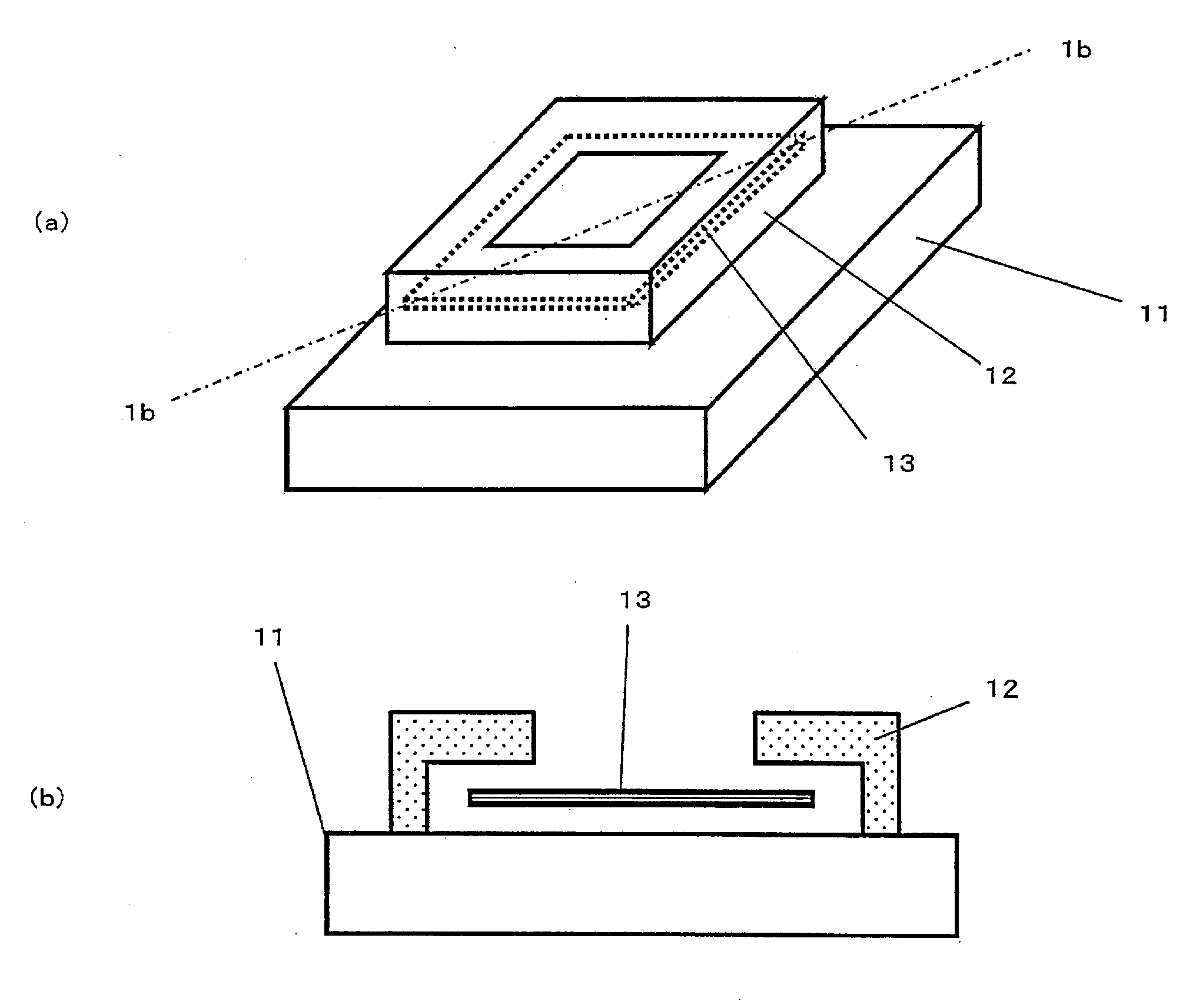
[0112]First, a schematic configuration for an electronic device according to this preferred embodiment will be described with reference to FIG. 1A, of which portion (a) is a perspective view illustrating a first preferred embodiment of the present invention and portion (b) is a cross-sectional view thereof as viewed on the plane 1b-1b shown in portion (a) of FIG. 1A.

[0113]As sho...

embodiment 2

[0223]Hereinafter, a second preferred embodiment of an electronic device according to the present invention will be described as an infrared sensor. In this preferred embodiment, the position of the heat sensing section 13 is controlled using the electrostatic force of electric charge that has been produced in the heat sensing section 13 as a result of electrostatic induction.

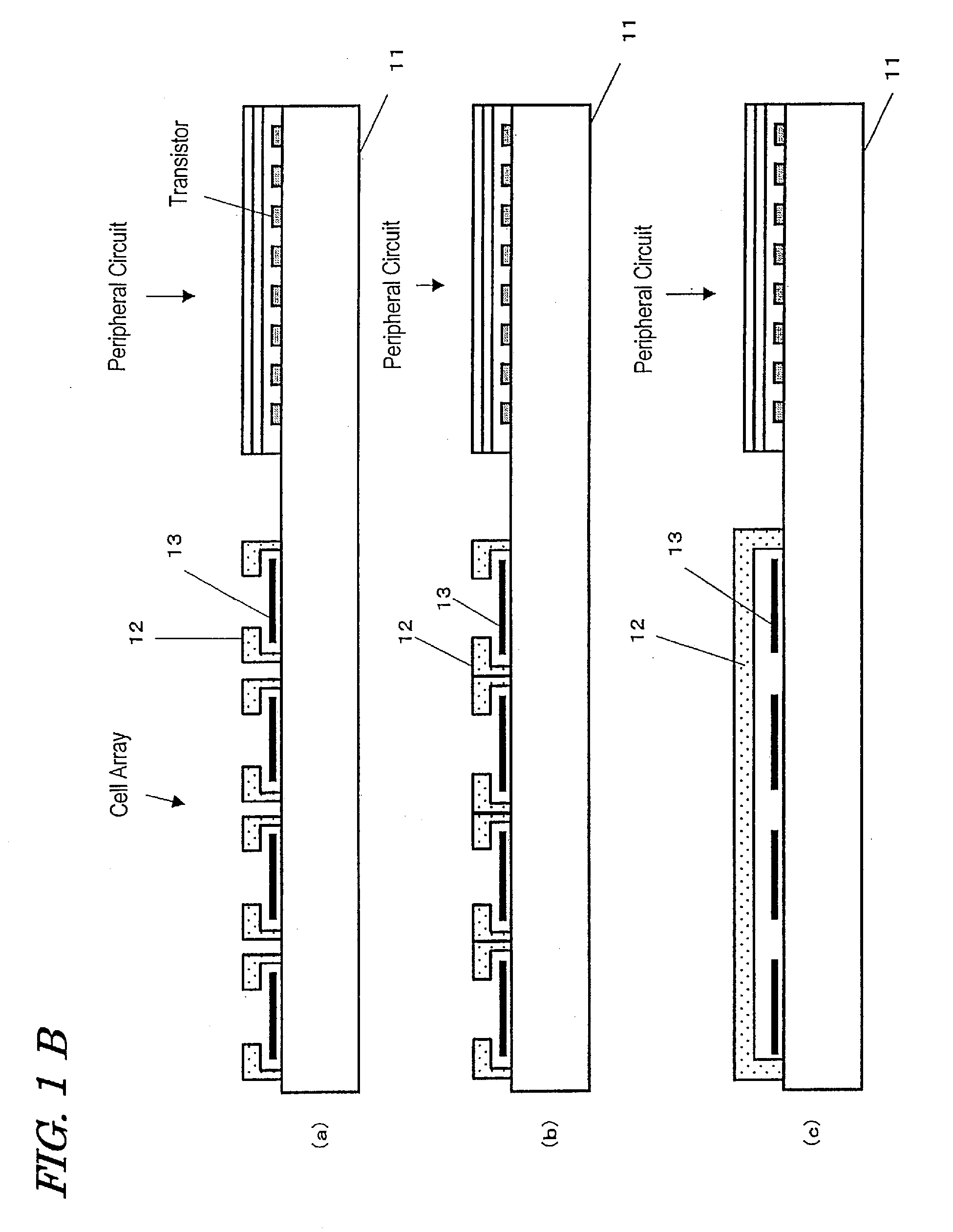
[0224]The overall configuration of the infrared sensor of this preferred embodiment is as shown in FIG. 1.

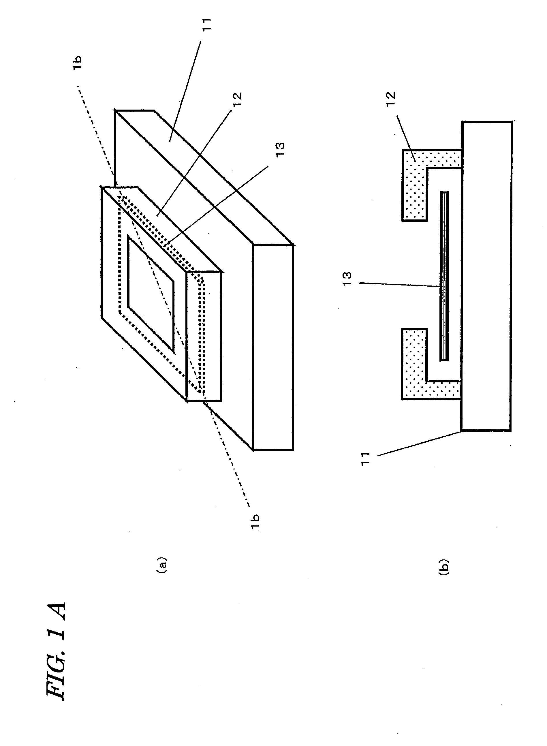
[0225]First of all, the configuration of the heat sensing section 13 of this preferred embodiment will be described with reference to FIG. 13. Specifically, FIG. 13(a) is a cross-sectional view as viewed on the plane 1b-1b shown in FIG. 1A, illustrating the configuration of the heat sensing section 13 in detail. FIG. 13(b) is a cross-sectional view as viewed on the plane 13b-13b shown in FIG. 13(a) and FIG. 13(c) is a cross-sectional view as viewed on the plane 13c-13c shown in FIG. 13(a).

[0226]As shown in ...

embodiment 3

[0234]Hereinafter, a third preferred embodiment of an electronic device according to the present invention will be described.

[0235]In this preferred embodiment, the position of the heat sensing section 13 is controlled using a magnetic field that has been generated by a coil arranged on the cavity wall portion 12 and an electromagnetic force that has been produced with respect to a magnetic body included in the heat sensing section.

[0236]The electronic device of this preferred embodiment also has the same overall configuration as that shown in FIG. 1 and also includes a heat sensing section 13, a cavity wall portion 12 and a substrate portion 11.

[0237]First of all, the configuration of the heat sensing section 13 of this preferred embodiment will be described with reference to FIG. 16. Specifically, FIG. 16(a) is a cross-sectional view as viewed on the plane 1b-1b shown in FIG. 1A, illustrating the configuration of the heat sensing section 13 in detail. FIG. 16(b) is a cross-section...


PUM

PropertyMeasurementUnit
wavelengthaaaaaaaaaa
thicknessaaaaaaaaaa
thicknessaaaaaaaaaa

Abstract

An electronic device according to the present invention includes: at least one heat sensing section (13), which includes a first contact portion (24) and of which a physical property varies responsive to an incoming infrared ray; a detector circuit section, which includes a second contact portion (42) and which senses the variation in the physical property of the heat sensing section (13); and a driving section (112), which is able to change a first state, in which the first and second contact portions (24, 42) are in contact with each other and electrically connected to each other, into a second state, in which the first and second contact portions (24, 42) are out of contact with each other and electrically disconnected from each other, and vice versa.

Description

[0001]This is a continuation of International Application No. PCT / JP2006 / 311113, with an international filing date of Jun. 2, 2006, which claims priority of Japanese Patent Application No. 2005-165560, filed on Jun. 6, 2005, the contents of which are hereby incorporated by reference.BACKGROUND OF THE INVENTION[0002]1. Field of the Invention[0003]The present invention relates to an electronic device and a method for fabricating an electronic device, and more particularly relates to a thermal infrared sensor and a thermal infrared image sensor.[0004]2. Description of the Related Art[0005]An infrared sensor for detecting an electromagnetic wave (or an infrared ray) with a wavelength of 3 μm to 10 μm has been used as a heat sensing sensor in crime prevention, measuring, remote sensing and various other fields of applications. An infrared image sensor, in which such sensors are arranged as a two-dimensional array, can obtain an even greater amount of information as a thermal image, and h...

Claims


Application Information

Patent Timeline
Patent Type & Authority Applications(United States)
IPC IPC(8): G01J5/00H01S4/00
CPCG01J5/02G01J5/024G01J5/0245G01J5/10Y10T29/49002G01J5/34H01L27/14669H01L31/02016H01L31/09G01J5/20
Inventor IKUSHIMA, KIMIYABABA, ASAKO
Owner PANASONIC CORP
Why Eureka
Try Eureka