Advanced hydrogenation of silicon solar cells

Active Publication Date: 2015-05-14
NEWSOUTH INNOVATIONS PTY LTD
View PDF2 Cites 10 Cited by
  • Summary
  • Abstract
  • Description
  • Claims
  • Application Information

AI Technical Summary

Benefits of technology

[0146]To maximise H0 generation, the Fermi level should be approximately 0.1 to 0.22 eV above mid-gap, depending on the temperature. For Fermi levels lower than this level, H+ is the dominant charge species of hydrogen whilst for Fermi levels higher than this level, H− is the dominant charge species of hydrogen. Ensuring a Fermi level of around this level allows a good penetration of hydrogen as H0 and H+ throughout the device. As shown in FIG. 10, for lightly doped n-type silicon such as the bulk doping density for n-type silicon solar cells typically in the range of 1×10¹⁵/cm3-1×1016/cm3 low temperatures can be used to achieve the desired Fermi level. However for n-type diffusions in silicon, the doping density is typically greater than 1×10¹⁹/cm3, and much higher temperatures must be used to obtain a Fermi level in the range of 0.1-0.22 eV above mid-gap.
[0147]If the emitter does not have to carry current then it may be optimised for hydrogen penetration, however if it does have to carry current then there is a trade-off between emitter sheet resistance and the temperature needed for effective hydrogenation.
[0148]Another approach is Tailoring of emitters to maximise H0 generation. If the junction is not required to carry current great distances (or not at all e.g. a front junction on a rear contact cell or a rear floating junction) then it may be tailored

Problems solved by technology

These lower the minority carrier lifetime of the silicon and therefore reduce the efficiencies of solar cells made from such material.
Failure of Existing Commercial Solar Cells to Capitalise on the Potential of Hydrogen Passivation
Currently, without a full understanding of the hydrogenation process and its potential, the designs of commercially manufactured solar cell structures are not ideal to facilitate hydrogenation throughout the cell, and this is reflected in the poor bulk lifetimes for technologies using standard commercial grade p-type wafers.
However these states in the respective polarity of silicon can lead to the neutralization of dopant atoms, and can no longer move throughout the silicon.
This behaviour of hydrogen in silicon has not been understood or has been overlooked in the past, with the result that attempts at hydrogenation have been less effective than would have been believed by cell designers.
The dissociation of the dopant-hydrogen complexes is difficult, as even if there is sufficient thermal energy to dissociate the complex, the Coulombic attraction between the dopant atom and the atomic hydrogen (H− for phosphorus and H+ for boron) prevents the escape of the hydrogen atom, and a rapid reformation of the dopant-hydrogen complex is likely.
It can now be seen that the main reasons for poor hydrogenation in the past include: heavy doping in emitters blocking hydrogen from penetrating deep within the silicon; absence of hydrogen sources from one or both surfaces; aluminium alloyed regions acting as sinks; failure to achieve the right charge state for the atoms of hydrogen to facilitate their bonding to certain types of defects and impurities; and no means of trapping of the hydrogen.
Conventional screen Printed Solar Cells dominate commercial manufacture however these have many features that limit the ability to hydrogenate the silicon properly.
Firstly, there is a hydrogen source on only one side of the wafer.
Another limitation is due to the metal-silicon interfaces, which are largely unshielded and so act as sinks that remove the hydrogen ions.
However they still suffer from the limi

Method used


Image

  • Advanced hydrogenation of silicon solar cells
  • Advanced hydrogenation of silicon solar cells
  • Advanced hydrogenation of silicon solar cells

Examples


application examples

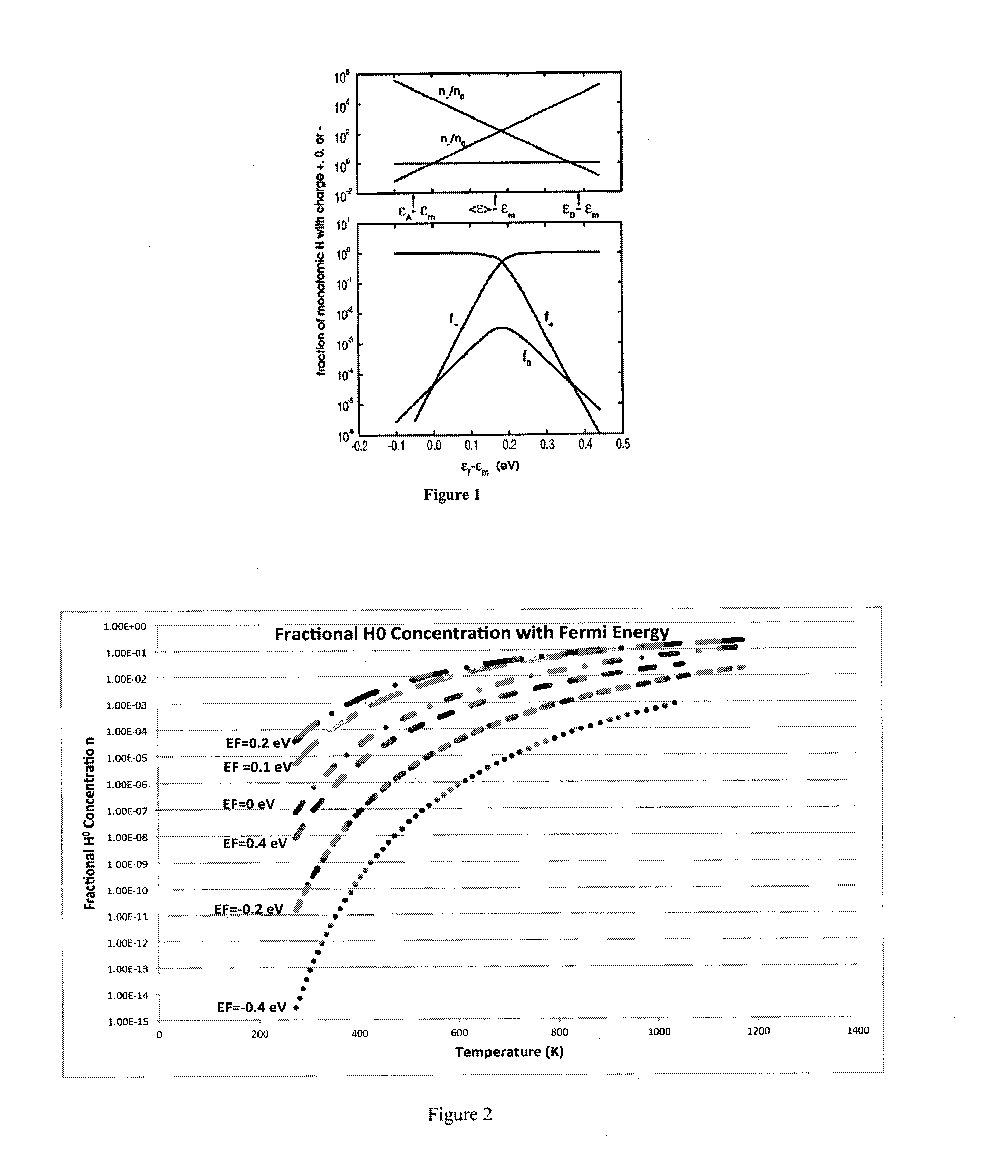
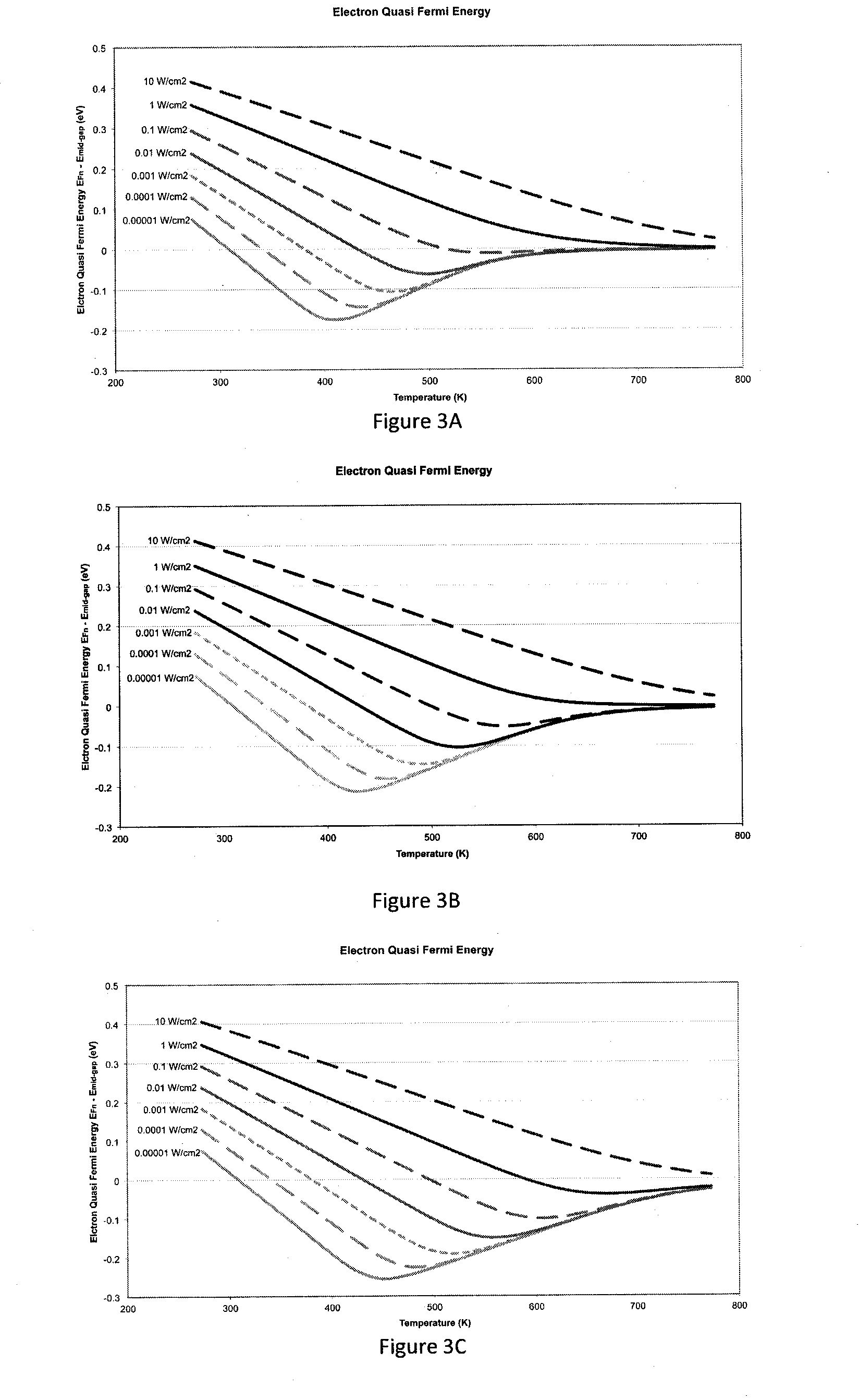
[0129]FIGS. 8, 9&10 graphically illustrate respectively fractional H0 concentration as a function of temperature and illumination for bulk p-type doping of 1.5×10¹⁶ with hydrogenation paths for material with a minority carrier lifetime of 100 microseconds; fractional H0 concentration and Electron Quasi Fermi Energy with low temperature hydrogenation paths for 1×10¹⁶ bulk doping with a minority carrier lifetime of 100 microseconds; and Fermi energies in n-type silicon (no illumination) as a function of doping concentration and temperature;

Post Anneal Cooling

[0130]At present hydrogen passivation is predominantly at 400° C. or carried out at relatively high temperatures (700° C. to 900° C.) when carried out in conjunction with metal firing processes. At these latter high temperatures, as long as the wafer is only lightly doped, the Fermi energy is nearly mid-bandgap for bulk material and the emitter Fermi energy is approaching 0.2 eV above midgap, so hydrogen may exist as H0 and hence ...

example 1

Standard High Temperature Hydrogenation Anneal with Constant Illumination During Cool Down

[0133]This method would consist of a high temperature anneal (˜700° C.) followed by a cool down with a constant illumination level sufficient to maintain the electron quasi Fermi energy above mid-gap at all times until the wafer has cooled enough for the next process. This may be carried out with any cooling rate, and one possible implementation would comprise incorporation of lights into the cooling region of an inline belt furnace.

example 2

Standard High Temperature Hydrogenation with Illumination Controlled Over Process

[0134]As above, the wafers would first be hydrogenated at high temperatures for a brief period with as much illumination as possible (up to a limit of several hundred suns). As the wafers cool the light intensity will also decrease such that the electron quasi-fermi energy remains in the ideal region for H0 generation (0.1-0.3 eV above mid bandgap). This may be achieved for example using a belt furnace where the light intensity is set to become weaker as the wafers progress through the cooling zone.


PUM


Abstract

A method of hydrogenation of a silicon photovoltaic junction device is provided, the silicon photovoltaic junction device comprising p-type silicon semiconductor material and n-type silicon semiconductor material forming at least one p-n junction.
The method comprises:
    • i) ensuring that any silicon surface phosphorus diffused layers through which hydrogen must diffuse have peak doping concentrations of 1×10²⁰ atoms/cm3 or less and silicon surface boron diffused layers through which hydrogen must diffuse have peak doping concentrations of 1×10¹⁹ atoms/cm3 or less;
    • ii) Providing one or more hydrogen sources accessible by each surface of the device; and
    • iii) Heating the device, or a local region of the device to at least 40° C. while simultaneously illuminating at least some and/or advantageously all of the device with at least one light source whereby the cumulative power of all the incident photons with sufficient energy to generate electron hole pairs within the silicon (in other words photons with energy levels above the bandgap of silicon of 1.12 eV) is at least 20 mW/cm2

Description

CROSS-REFERENCE TO RELATED APPLICATIONS[0001]This application is a division of application Ser. No. 14 / 402,654 filed Nov. 20, 2014 for “Advanced Hydrogenation of Silicon Solar Cells”, which claims priority from PCT International Patent Application No. PCT / AU2013 / 00528, filed May 20, 2013 and Australian Patent Application No. 2012902090, filed May 21, 2012, which are hereby incorporated by reference herein.INTRODUCTION[0002]The present invention relates generally to the manufacture of silicon solar cells and in particular the invention provides a new method of hydrogenation for silicon solar cells.BACKGROUND[0003]Hydrogenation of crystalline silicon involves the bonding of hydrogen atoms to crystallographic defects or contamination within the silicon lattice in a way that prevents that defect or contaminant from acting as a recombination site for minority carriers. This is known as passivation of the particular recombination site. This is important for semiconductor devices that requ...

Claims


Application Information

Patent Timeline
IPC IPC(8): H01L31/18
CPCH01L31/1804H01L31/1868H01L21/3003H01L31/1864Y02E10/547Y02P70/50H01L21/67109H01L21/67115H01L21/67706H01L31/186Y02B10/10Y02E10/50
Inventor WENHAM, STUART ROSSHAMER, PHILLIP GEORGEHALLAM, BRETT JASONSUGIANTO, ADELINECHAN, CATHERINE EMILYSONG, LIHUILU, PEI HSUANWENHAM, ALISON MAREEMAI, LYCHONG, CHEE MUNXU, GUANGQIEDWARDS, MATTHEW
Owner NEWSOUTH INNOVATIONS PTY LTD
Why Eureka
Try Eureka