Closed trench MOSFET with floating trench rings as termination

a technology of trench rings and mosfet cells, which is applied in the direction of solid-state devices, transistors, electrical devices, etc., can solve the problems of reducing the performance of the device, reducing the drain to source resistance of the cell, and affecting so as to improve the performance of the semiconductor power device, and reduce the source to drain resistance rds

Active Publication Date: 2008-07-31
FORCE MOS TECH CO LTD
View PDF9 Cites 87 Cited by
  • Summary
  • Abstract
  • Description
  • Claims
  • Application Information

AI Technical Summary

Benefits of technology

[0008]Another aspect of the present invention is configure the MOSFET device with closed MOSFET cell wherein the source regions are disposed at a distance away from the wider trench gate for gate metal contact and from the device corners and edges, and are also disposed away from the termination areas thus the ruggedness of the device is improved.
[0014]This invention further discloses a method of manufacturing a semiconductor power device. The method includes a step of forming a plurality of closed power transistor cells each surrounded by trenched gates constituting substantially a square or rectangular shaped cell in an active area and applying a source mask for covering a gate-pad area above wider trenched gates whereby source regions are formed in the closed power transistor cells in the active area and blocked from the gate pad area. In an exemplary embodiment, the step of applying a source mask for implanting a source region further comprising a step of applying the source mask for covering a termination area opposite the active area. In another exemplary embodiment, the step of applying a source mask for implanting a source region further comprising a step of applying the source mask for implanting the source region at a distance away from corners of edges of the semiconductor power device. In another exemplary embodiment, the method further includes a step of disposing a source contact substantially at a center portion of the closed cell by opening a source-body contact trench in an insulation layer covering the closed semiconductor power device and extending the source-body contact trench into a source region below the insulation layer and into a body region below the source region and filling the source body contract trench with a source contact plug. In another exemplary embodiment, the method further includes a step of disposing a source metal layer above the insulation layer to electrically contact the source contact plug. In another exemplary embodiment, the step of forming the plurality of closed power transistor cells comprising a step of forming the closed power transistor cells as closed N-channel MOSFET cells on a red phosphorous substrate. In another exemplary embodiment, the step of forming a plurality of closed power transistor cells by forming the trenched gates surrounding the closed power transistor cells further comprising a step of forming a plurality of trenched rings for connecting to a floating potential whereby a breakdown voltage of the semiconductor power device is improved.

Problems solved by technology

The design and cell configurations to accomplish such requirements become more challenges to those of ordinary skill in the art, particularly when the cell density of the semiconductor power device is increased to a cell density that is above and beyond 600 M / in2 (six hundred million cells per square inch).
The configuration as disclosed however has the disadvantages due to the fact that the stripe cells have higher drain to source resistance (Rds) than the closed cells.
Furthermore, the three-mask process allows a n+ region to locate in the termination area and the trench gate area and such configuration degrades the device ruggedness due the fact of additional latch-up of doped zones to become the parasitic N+PN bipolar transistors.
When the device turns on, the active cells near the trench gates will be turned on first that can easily trigger the parasitic N+PN to cause potential damages to the device.
The corners of the cells are particular vulnerable to such inadvertent triggering-on of the parasitic N+PN transistors due to the higher electrical field around the corner regions of the cells.
Such techniques are required due the damages found near the device corners during a voltage surge with unclamped inductance switching (UIS) when a device is provided with such dummy cells as damage preventive structures.
The disclosures made in this patent have further disadvantages arising from the process flow with the formation of the n+ and P-body before the trench gate formation.
A punch-through problem is not preventable for a device with cell density that is higher than 112 million cells per square inch, i.e., as the device pitch is reduced to 2.4 um.
The punch through issue arises due to the boron segregation during sacrificial oxidation and gate oxidation.

Method used


Image

  • Closed trench MOSFET with floating trench rings as termination
  • Closed trench MOSFET with floating trench rings as termination
  • Closed trench MOSFET with floating trench rings as termination

Examples


Embodiment Construction

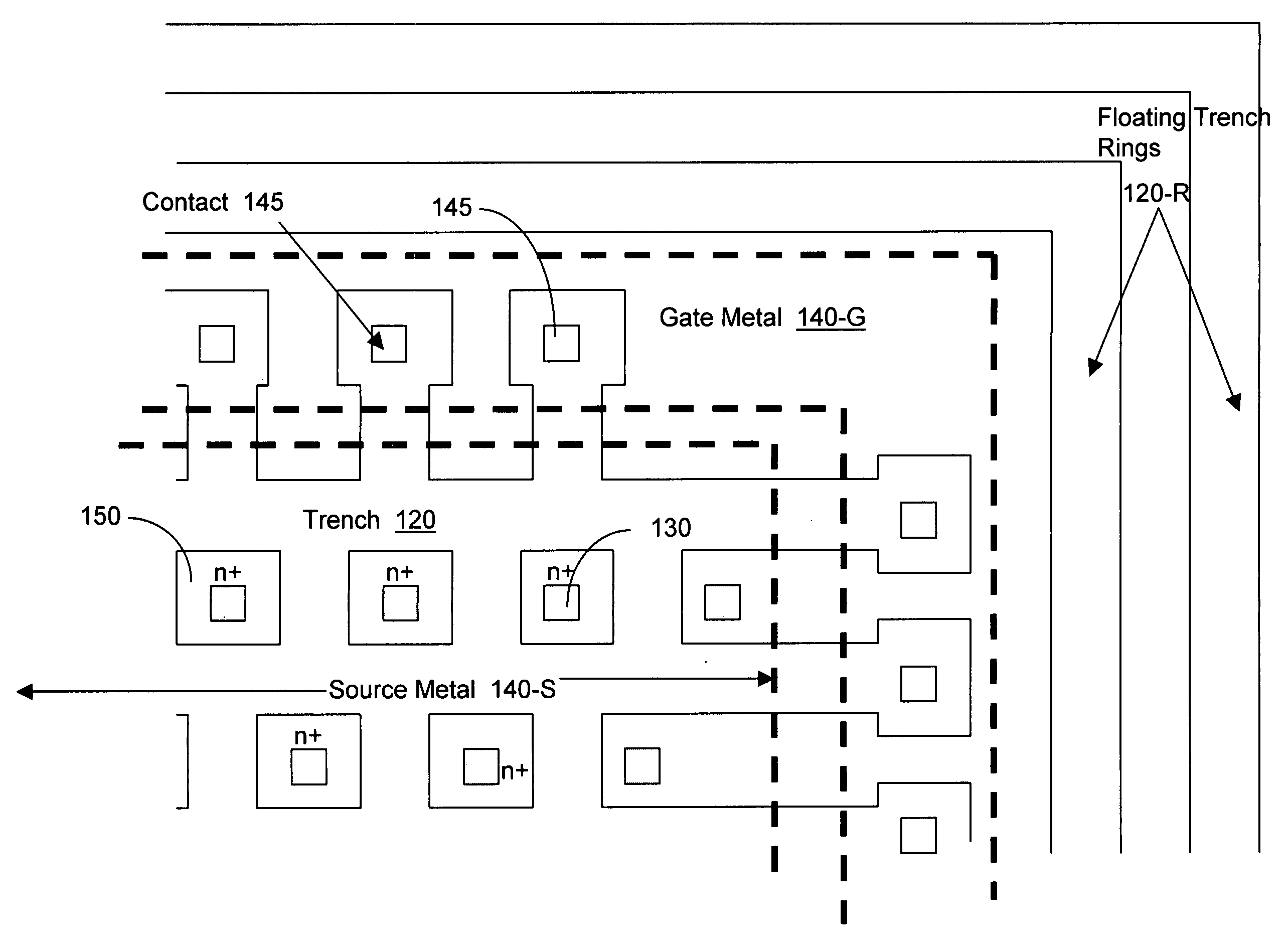
[0023]Please refer to FIGS. 2A to 2B for an exemplary embodiment of this invention where a metal oxide semiconductor field effect transistor (MOSFET) device 100 is supported on a substrate 105 formed with an epitaxial layer 110. The MOSFET device 100 includes a trenched gate 120 disposed in a trench with a gate insulation layer 115 formed over the walls of the trench. A body region 125 that is doped with a dopant of second conductivity type, e.g., P-type dopant, extends between the trenched gates 120. The P-body regions 125 encompassing a source region 130 doped with the dopant of first conductivity, e.g., N+ dopant. The source regions 130 are formed near the top surface of the epitaxial layer surrounding the trenched gates 120. The top surface of the semiconductor substrate extending over the top of the trenched gate, the P body regions 125 and the source regions 130 are covered with a NSG and a BPSG protective layers 135. A source metal layer 140-S and gate metal layer 140-G are f...


PUM


Abstract

A semiconductor power device includes a plurality of closed N-channel MOSFET cells surrounded by trenched gates constituting substantially a square or rectangular cell. The trenched gates are further extended to a gate contact area and having greater width as wider trenched gates for electrically contacting a gate pad wherein the semiconductor power device further includes a source region disposed only in regions near the trenched gates in the closed N-channel MOSFET cells and away from regions near the wider trenched gate whereby a device ruggedness is improved. The source region is further disposed at a distance away from a corner or an edge of the semiconductor power device and away from a termination area. The semiconductor device further includes multiple trenched rings disposed in a termination area opposite the active area and the trenched rings having a floating voltage. The closed N-channel MOSFET cells are further supported on a red phosphorous substrate.

Description

BACKGROUND OF THE INVENTION[0001]1. Field of the Invention[0002]This invention relates generally to the cell structure, device configuration and fabrication process of power semiconductor devices. More particularly, this invention relates to a novel and improved cell structure, device configuration and improved process for fabricating a trenched semiconductor power device to achieve reduced source to drain resistance Rds, improved device ruggedness and breakdown voltage.[0003]2. Description of the Related Art[0004]As the cell density of the semiconductor power devices increases, there is a greater need to provide configuration such that the source to drain resistance Rsd can be reduced. Meanwhile, in order to provide power devices with broader spectrum of applications, the reduction of Rds, however must be achieved without comprising the device ruggedness and the breakdown voltage. The design and cell configurations to accomplish such requirements become more challenges to those of ...

Claims


Application Information

Patent Timeline
Patent Type & Authority Applications(United States)
IPC IPC(8): H01L27/088H01L21/8234
CPCH01L21/823418H01L21/823437H01L27/088H01L29/0696H01L29/407H01L29/41766H01L29/7813H01L29/456H01L29/4941H01L29/66727H01L29/66734H01L29/7811H01L29/4238
Inventor HSHIEH, FWU-IUAN
Owner FORCE MOS TECH CO LTD
Why Eureka
Try Eureka