Internal balanced coil for inductively coupled high density plasma processing chamber

a plasma processing chamber and inductively coupled technology, applied in the direction of electrostatic charges, coatings, electric discharge lamps, etc., can solve the problems of difficult to completely fill the high-aspect-ratio gap using conventional cvd techniques, the gapfilling ability is relatively poor, and the number of persistent challenges in achieving the desired deposition property

Inactive Publication Date: 2008-08-07
APPLIED MATERIALS INC
View PDF12 Cites 47 Cited by
  • Summary
  • Abstract
  • Description
  • Claims
  • Application Information

AI Technical Summary

Benefits of technology

[0001]The present invention relates generally to the field of semiconductor processing equipment. More particularly, the present invention relates to methods and apparatus for generating plasma, for e

Problems solved by technology

One persistent challenge faced by semiconductor manufacturers in the design and fabrication of such densely packed integrated circuits is the desire to prevent spurious interactions between circuit elements, a goal that has required ongoing innovation as geometry scales continue to decrease.
High-aspect-ratio gaps are difficult to fill completely using conventional CVD techniques, which tend to have relatively poor gapfill abilities.
Even with the use of HDP and ICP processes, there remain a number of persistent challenges in achieving desired deposition properties.
These include the need to manage thermal characteristics of the plasma within a processing chamber, particularly with high-energy processes that may result in te

Method used


Image

  • Internal balanced coil for inductively coupled high density plasma processing chamber
  • Internal balanced coil for inductively coupled high density plasma processing chamber
  • Internal balanced coil for inductively coupled high density plasma processing chamber

Examples


Embodiment Construction

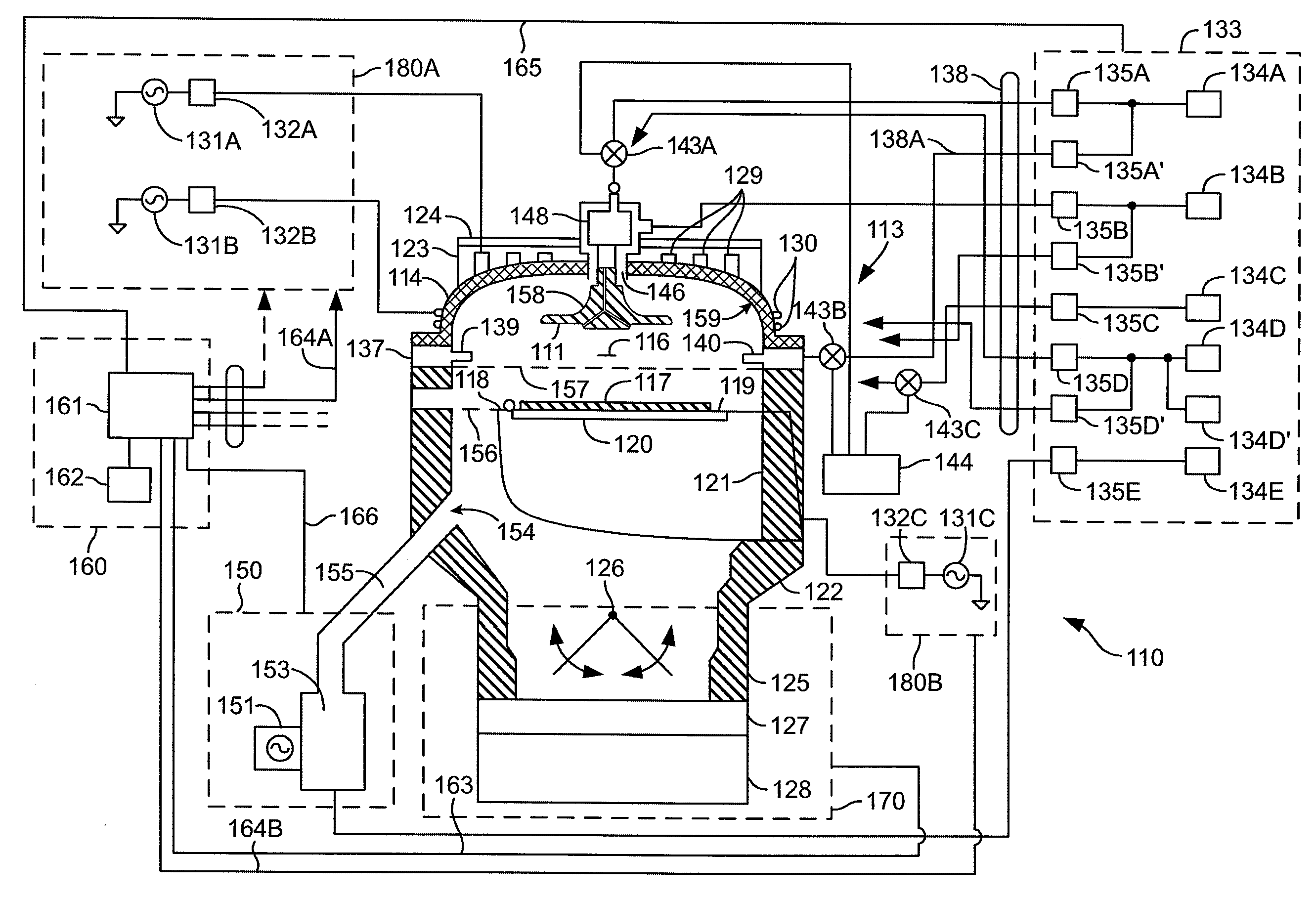
[0041]The present invention relates generally to the field of semiconductor processing equipment. More particularly, the present invention relates to methods and apparatus for generating plasma, for example coils, used with high density plasma deposition chambers. The methods and apparatus can be applied to other semiconductor processes, for example etch processes used to form integrated circuits.

[0042]1. Exemplary ICP Chamber

[0043]Embodiments of the present invention use systems manufactured by APPLIED MATERIALS, INC., of Santa Clara, Calif., a general description of which is provided in commonly assigned U.S. Pat. Nos. 5,994,662; 6,170,428; and 6,450,117; and U.S. patent application Ser. Nos. 10 / 963,030 and 11 / 075,527; the entire disclosures of these patents and applications are incorporated herein by reference. An overview of the ICP reactor is provided in connection with FIG. 1. FIG. 1 schematically illustrates the structure of an exemplary HDP-CVD system 110 in one embodiment. ...


PUM

PropertyMeasurementUnit
Lengthaaaaaaaaaa
Electrical inductanceaaaaaaaaaa
Electric potential / voltageaaaaaaaaaa

Abstract

A coil is provided for use in a semiconductor processing system to generate a plasma with a magnetic field in a chamber. The coil comprises a first coil segment, a second coil segment and an internal balance capacitor. The first coils segment has a first end and a second end. The first end of the coil segment is adapted to connect to a power source. The second coil segment has a first and second end. The second end of the first coil segment is adapted to connect to an external balance capacitor. The internal balance capacitor is connected in series between the second end of the first coil segment and the first end of the second coil segment. The internal balance capacitor and the coil segments are adapted to provide a voltage peak along the first coil segment substantially aligned with a virtual ground along the second coil segment.

Description

BACKGROUND OF THE INVENTION[0001]The present invention relates generally to the field of semiconductor processing equipment. More particularly, the present invention relates to methods and apparatus for generating plasma, for example coils, used with high density plasma deposition chambers. The methods and apparatus can be applied to other semiconductor processes, for example etch processes used to form integrated circuits.[0002]One of the primary steps in the fabrication of modern semiconductor devices is the formation of a film, such as a silicon oxide film, on a semiconductor substrate. Silicon oxide is widely used as an electrically insulating dielectric layer in the manufacture of semiconductor devices. As is well known, a silicon oxide film can be deposited by a thermal chemical-vapor deposition (“CVD”) process or by a plasma-enhanced chemical-vapor deposition (“PECVD”) process. In a conventional thermal CVD process, reactive gases are supplied to a surface of the substrate, w...

Claims


Application Information

Patent Timeline
IPC IPC(8): H01L21/3065C23C16/00H05F3/00
CPCH01J37/321
Inventor CHEN, ROBERTLAI, CANFENGCHEN, XINGLONGLUO, WEIYIHUA, ZHONG QIANGLU, SIQINGRASHEED, MUHAMMADLIANG, QIWEILUBOMIRSKY, DMITRYYIEH, ELLIE Y.
Owner APPLIED MATERIALS INC
Why Eureka
Try Eureka