Non-volatile semiconductor memory device

a non-volatile, semiconductor technology, applied in semiconductor devices, digital storage, instruments, etc., can solve the problems of difficult improvement of program throughput, difficulty in inability to increase the number of memory cells at the time of program operation. to achieve the effect of effectively controlling suppressing and reducing program disturbance, improving the disturb margin, and reducing the voltage difference between drain voltag

Inactive Publication Date: 2008-08-07
GENUSION
View PDF11 Cites 12 Cited by
  • Summary
  • Abstract
  • Description
  • Claims
  • Application Information

AI Technical Summary

Benefits of technology

[0044]According to the present invention, in the non-volatile semiconductor memory device, even at the time when a voltage between the source and the drain of a memory cell transistor which is to be programmed is lowered, it is possible to set the drain voltage of a non-programming memory cell higher than Vcc. Therefore, it is possible to make the voltage difference between the drain voltage of the memory cell transistor which is to be programmed and the drain voltage of the non-programming memory cell, greater. As a result, in the non-volatile semiconductor memory device, it is possible to improve the disturb margin at the time of programming. Also, because it is possible to control the voltage between the source and drain of a memory cell transistor it is also possible to realize the miniaturization of the gate length direction of a memory cell transistor.
[0045]In addition, according to this invention, by making the construction of the source side into a construction where, compared to the drain side, it is difficult to program, it is possible to effectively control suppress and reduce program disturbance which occurs on the source side.

Problems solved by technology

However, the number of memory cells which could be simultaneously programmed in a program operation by CHE injection could not be increased.
The number of memory cells at the time of program operation could not be increased due to a memory cell current which flowed at a few hundred μA and it was difficult to improve a program throughput.
And with the application of the high voltage, a problem is created where there is limit to the miniaturization of a gate length direction.
However, the problem of disturbance is likely to occur in the unselected memory cell transistor during program operation.
The problem of disturbance occurs particularly on the memory cell transistor which is connected to an unselected bit line and a selected word line.
There is a great danger that a disturbance problem will occur in the memory cell transistors MCn0b, MCn1a, MCn1b .
A disturbance problem occurs when the drain voltage of the unselected memory cell transistor MCn1a which connected to the same selection gate SGa and is connected to the sub bit line SBL1a is at Vcc.
Here, if the drain voltage Vcc of the memory cell transistor MCn1a, which is not to be programmed, is a low voltage, then a problem occurs where selectivity becomes worse.
The same disturbance problem as the drain occurs in the source side.
Therefore, disturbance characteristics are not sufficient.
However, when a method of charging by a high voltage from the side of the main bit line MBL is adopted, a loss in consumption energy and high voltage setup time occurs.
Also, according to this method, in the case where a main / sub bit line construction is adopted in which a plurality of sub bit lines SBL are connected to one main bit line MBL as shown in FIG. 1, a problem occurs whereby the above stated voltage cannot be applied to the cell connected to the same main bit line MBL.

Method used


Image

  • Non-volatile semiconductor memory device
  • Non-volatile semiconductor memory device
  • Non-volatile semiconductor memory device

Examples


first embodiment

[0078]The non-volatile semiconductor device relating to a first embodiment will be explained by referring to FIG. 4A to FIG. 6.

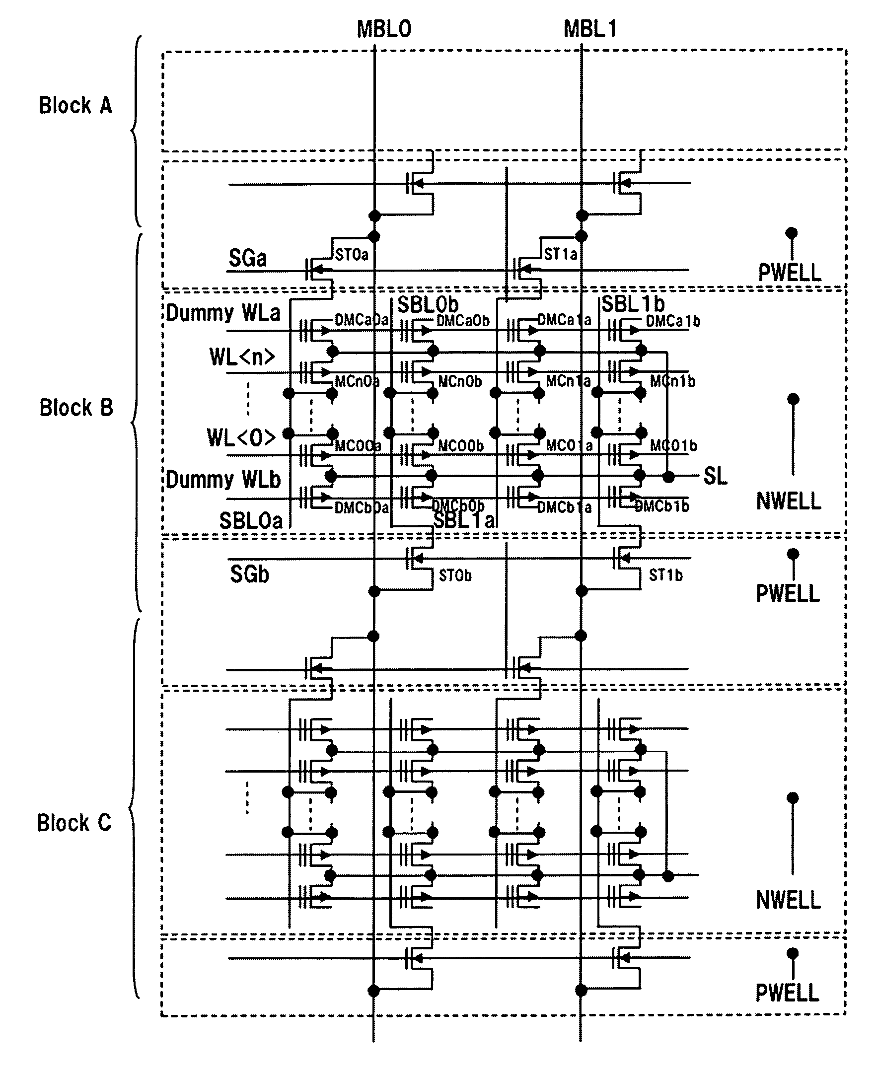
[0079]FIG. 4A is a circuit diagram which shows plural blocks, especially a Block B which is in adjacent to Blocks A and C, in the non-volatile semiconductor memory device of the first embodiment.

[0080]FIG. 4B shows a block diagram of the non-volatile semiconductor memory device of the first embodiment. As shown in FIG. 4B, the memory device includes a Charge Pump Circuits for generating VPwl, VPuwl, VPnwell from externally supplied Vcc; an Address Decoders for receiving externally supplied address signals and for decoding them to supply the decoded selection signals; a WL / SG / SL / Well Drivers for receiving the decoded selection signals and for driving word lines, selection gates, source lines and wells; a Bit Line Control Circuits for selectively supplying data (“0” or “1”) to main bit lines; and a memory cell array having the Blocks described in FIG. 4A.

[0081...

second embodiment

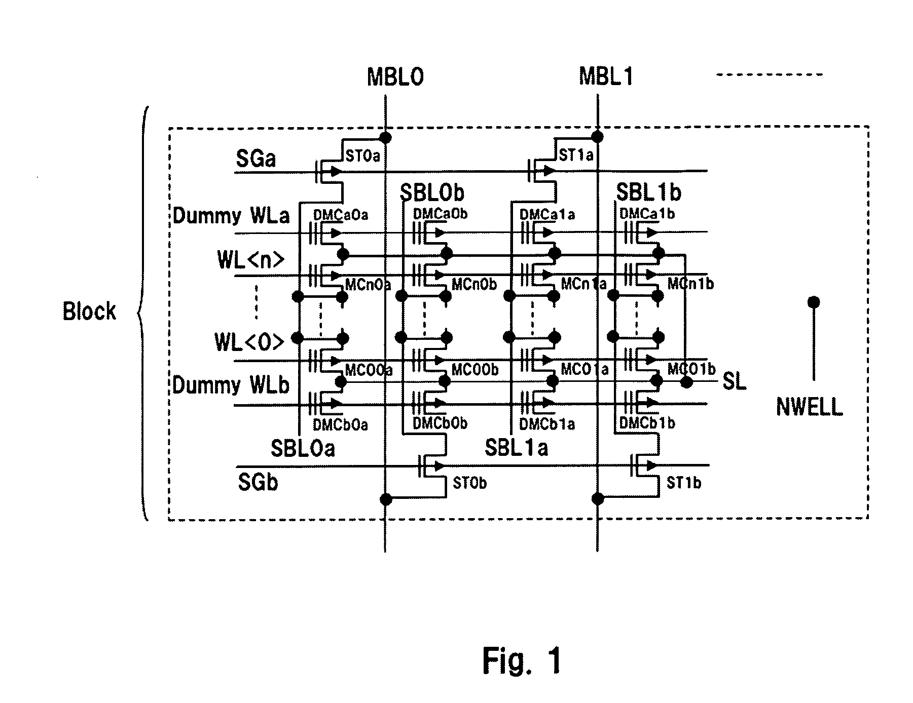
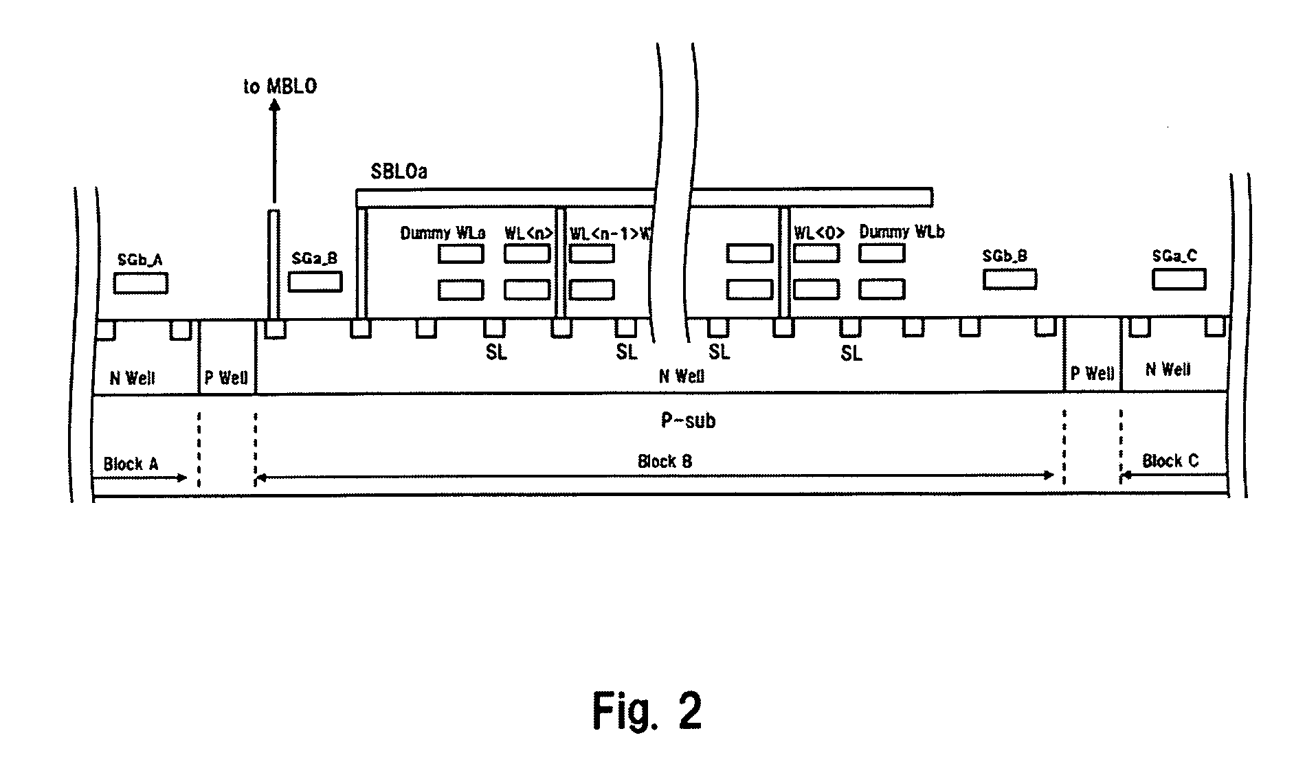
[0099]FIGS. 8B and 8C are plan view of the layout of patterns. Also in the second embodiment, it is preferred to have the local interconnections as described in FIG. 5D.

[0100]Further, as is shown in FIG. 8A, in the present embodiment, in the memory cells MC00a, . . . , MCn0a, MC00b, . . . , MCn0b, MC01a, . . . , MCna, MC01b, MCn1b . . . floating gates are formed on insulation layers above the channel regions. The word lines WL0>, . . . , WL which are control gates, are formed above these floating gates. In addition, in the present embodiment, floating gates are formed on insulation layers above the channel regions of the selection transistors ST0a, ST1a, ST0b, ST1b . . . Further, the selection gates SG1A, SG0B, SG1B, SG0C, . . . which also are control gates, are formed above the floating gates. Here, as stated above, the floating gates and selection gates in the selection transistors ST0a, ST1a, ST0b, ST1b are electrically connected.

[0101]Next, a timing control at the time of progra...


PUM


Abstract

According to an one aspect of the present invention, it is provided a non-volatile semiconductor memory device comprising: a first N type well; a plurality of P type non-volatile memory cells arranged in matrix and formed in the N type well; a plurality of sub-bit lines, each of the sub-bit lines being connected to drains of the P type non-volatile memory cells in a respective one of columns of the matrix; a first P type well; and a plurality of N type selection transistors, each of the selection transistors selectively connecting a respective one of sub-bit lines to a corresponding one of main bit lines.

Description

FIELD OF THE INVENTION[0001]This invention relates to an electrically programmable and erasable non-volatile semiconductor memory device.BACKGROUND OF THE INVENTION[0002]Conventionally, a NAND type flash memory and a NOR type flash memory which can program and erase, are widely adopted in a non-volatile semiconductor memory device. Recently, there have been greater demands for an increase in speed of the program operation in not only a NAND type flash memory but also in a NOR type flash memory. In a conventional NOR type flash memory, an N channel type transistor is adopted. The N channel type transistor of the NOR type flash memory conducts a program operation by CHE (Channel Hot Electron) injection. However, the number of memory cells which could be simultaneously programmed in a program operation by CHE injection could not be increased. The number of memory cells at the time of program operation could not be increased due to a memory cell current which flowed at a few hundred μA ...

Claims


Application Information

Patent Timeline
Patent Type & Authority Applications(United States)
IPC IPC(8): G11C16/04
CPCG11C16/0416H01L27/11524H01L27/11521H01L27/115H10B41/35H10B69/00H10B41/30
Inventor OGURA, TAKUAJIKA, NATSUO
Owner GENUSION
Why Eureka
Try Eureka