Nonvolatile semiconductor memory device with advanced multi-page program operation

a nonvolatile, multi-page technology, applied in the direction of memory address/allocation/relocation, instruments, computing, etc., can solve the problems of fast read and write speed of the device, loss of contents stored in memory cells, erase and write (or program) operations that cannot be executed through the electronic system itself, etc., to achieve the effect of reducing the programming tim

Active Publication Date: 2008-08-07
SAMSUNG ELECTRONICS CO LTD
View PDF14 Cites 33 Cited by
  • Summary
  • Abstract
  • Description
  • Claims
  • Application Information

AI Technical Summary

Benefits of technology

[0020]Exemplary embodiments of the present invention are directed to a nonvolatile semiconductor memory device capable of reducing programming time without increasing a unit of program of a multilevel flash memory. In an exemplary embodiment, a nonvolatile semiconductor memory device for performing a programming of multilevel data includes a memory cell array having a plurality of banks, each including a cache block, and a plurality of page buffer. The page buffer corresponds to each of the plu

Problems solved by technology

The volatile semiconductor memory device is fast in read and write speed, but has a shortcoming that contents stored in memory cells are lost when an external power supply is cut off.
However, in the MROM, PROM, and EPROM, erase and write (or program) o

Method used


Image

  • Nonvolatile semiconductor memory device with advanced multi-page program operation
  • Nonvolatile semiconductor memory device with advanced multi-page program operation
  • Nonvolatile semiconductor memory device with advanced multi-page program operation

Examples


Embodiment Construction

[0026]The present invention will now be described more fully hereinafter with reference to the accompanying drawings, in which preferred embodiments of the invention are shown. This invention, however, may be embodied in many different forms and should not be construed as limited to the embodiments set forth herein. Rather, these embodiments are provided so that this disclosure will be thorough and complete, and will fully convey the scope of the invention to those skilled in the art. In the drawings, like numbers refer to like elements throughout.

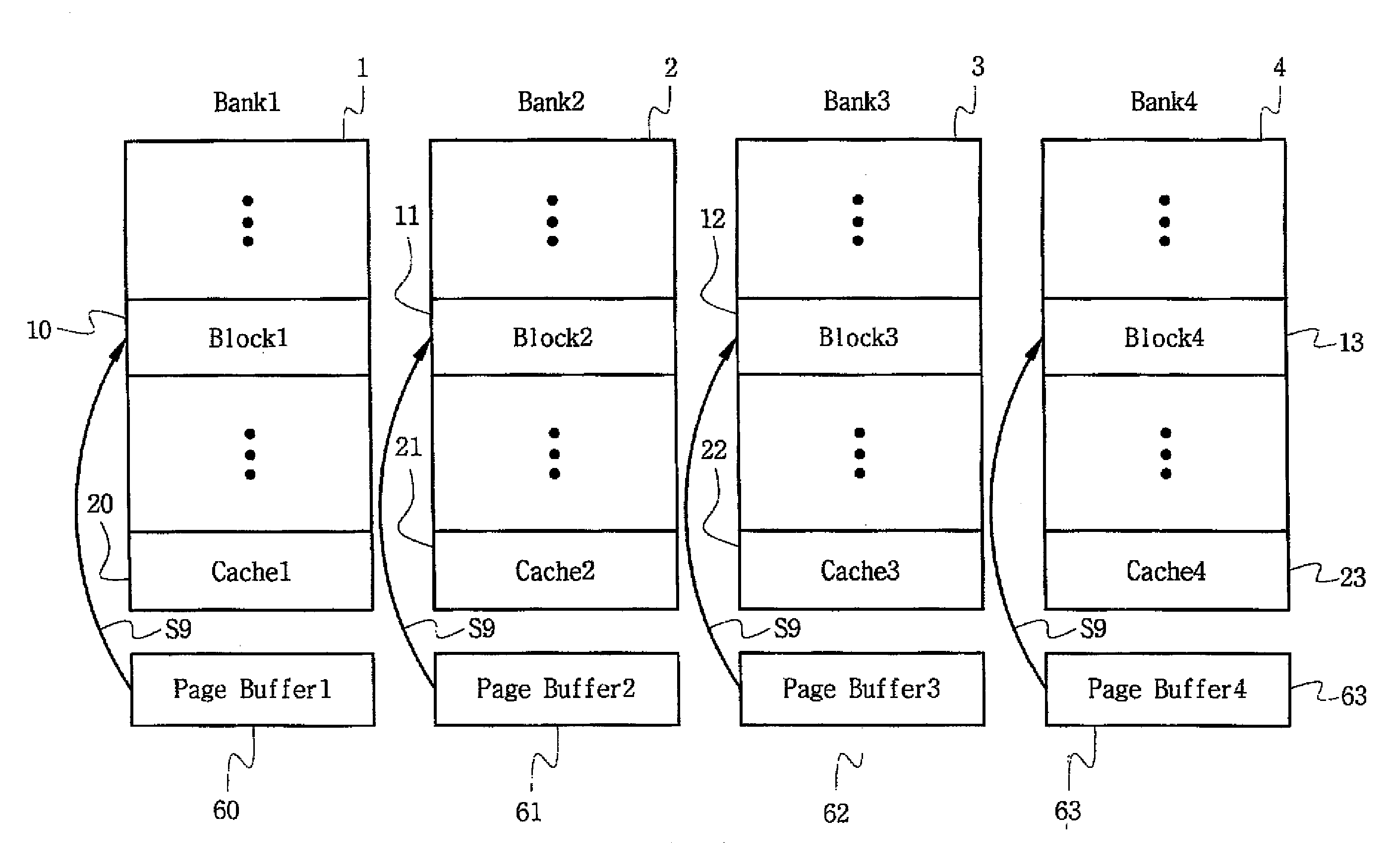
[0027]According to an embodiment of the invention a cache block having a predetermined data storage capacity is adapted in each bank of a memory cell array to reduce programming time without increasing a unit of program as compared to a conventional program scheme. A programming circuit sequentially performs an operation of loading page data into a corresponding page buffer and an operation of programming the loaded page data into a corres...


PUM


Abstract

A nonvolatile semiconductor memory device for an efficient program of multilevel data includes a memory cell array having a plurality of banks and a cache block corresponding to each of the plurality of banks. The cache block has a predetermined data storage capacity. A page buffer is included which corresponds to each of the plurality of banks. A programming circuit programs all of the plurality of banks except a last of said banks with page data. The page data is loaded through each page buffer and programmed into each cache block such that when page data for the last bank is loaded into the page buffer, the loaded page data and the page data programmed into the respective cache blocks are programmed into respective corresponding banks. Accordingly, the time taken in programming can be reduced without increasing a unit of program in a multilevel flash memory, thereby improving performance in a multilevel program of a nonvolatile semiconductor memory device.

Description

CROSS-REFERENCE TO RELATED APPLICATION[0001]This U.S. non-provisional patent application claims priority under 35 U.S.C. §119 of Korean Patent Application 10-2007-0012039 filed on Feb. 6, 2007, the entire contents of which are hereby incorporated by reference in its entirety.BACKGROUND OF THE INVENTION[0002]1. Field of the Invention[0003]Embodiments of the invention relate to nonvolatile semiconductor memories. More particularly, embodiments of the invention relate to a multilevel nonvolatile semiconductor memory capable of storing data of two or more bits in one memory cell.[0004]2. Description of the Related Art[0005]A recently rapid development of information processing apparatuses such as a computer, etc. tends to bring about a high-speed operation and large capacity in semiconductor memory devices employed as main components of the information processing apparatuses.[0006]Typically a semiconductor memory device may be largely classified as a volatile semiconductor memory device...

Claims


Application Information

Patent Timeline
IPC IPC(8): G06F12/02G06F12/08
CPCG06F2212/7203G06F12/0246G11C16/04G11C16/06G11C16/10
Inventor CHAE, DONG-HYUKLIM, YOUNG-HO
Owner SAMSUNG ELECTRONICS CO LTD
Why Eureka
Try Eureka