Nanowire heterostructures

a nanowire and heterostructure technology, applied in the field of nanowire heterostructures, can solve the problems of inhibiting the conductance or transconductance measurement of the nanowire, and affecting the performance of the nanowir

Active Publication Date: 2008-08-14
PRESIDENT & FELLOWS OF HARVARD COLLEGE
View PDF99 Cites 97 Cited by
  • Summary
  • Abstract
  • Description
  • Claims
  • Application Information

AI Technical Summary

Problems solved by technology

However, the metal-semiconductor junction between the electrode and the nanowire creates a Schottky barrier, which inhibits conductance or transconductance measurements of the nanowire or otherwise impedes its performance.
While Schottky barriers can be reduced by increasing dopant concentrations within the semiconductor nanowire, such increases in dopant concentrations will generally reduce the mobility of the charge carriers within the nanoscale wire, which can impede the performance of the nanowire.
However, reducing dopant concentrations within the semiconductor nanowire will reduce the number of available charge carriers within the nanoscale wire, and it would be expected by those of ordinary skill in the art that such a reduction in dopant concentration would decrease the conductivity of the nanowire, ultimately rendering it an insulator if no charge carriers are present.

Method used


Image

  • Nanowire heterostructures
  • Nanowire heterostructures
  • Nanowire heterostructures

Examples


example 1

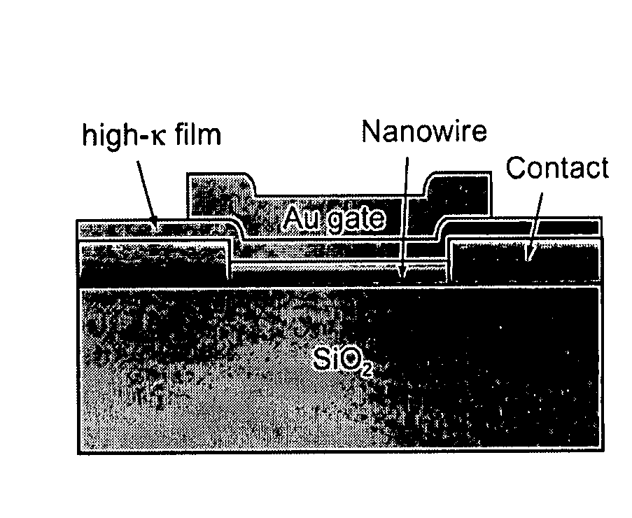
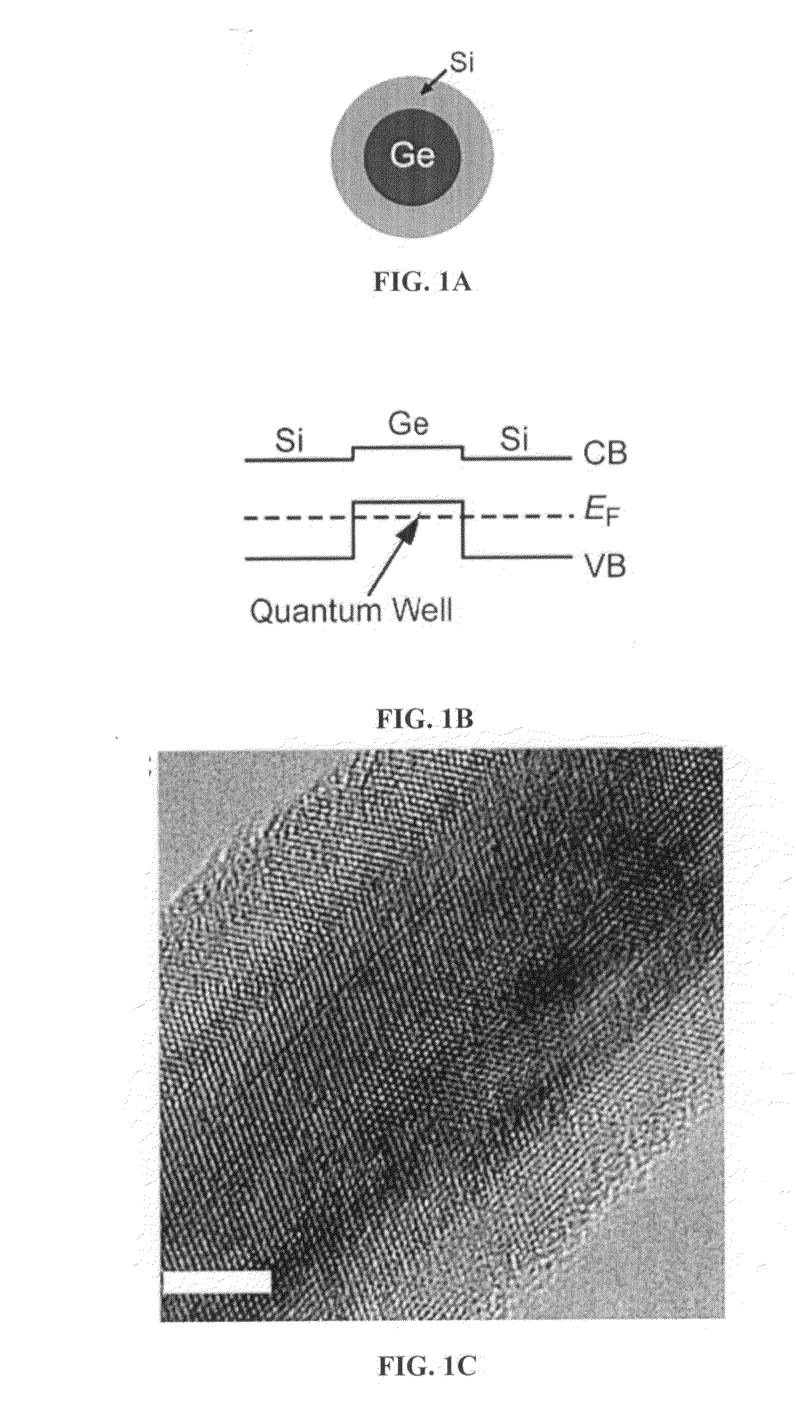
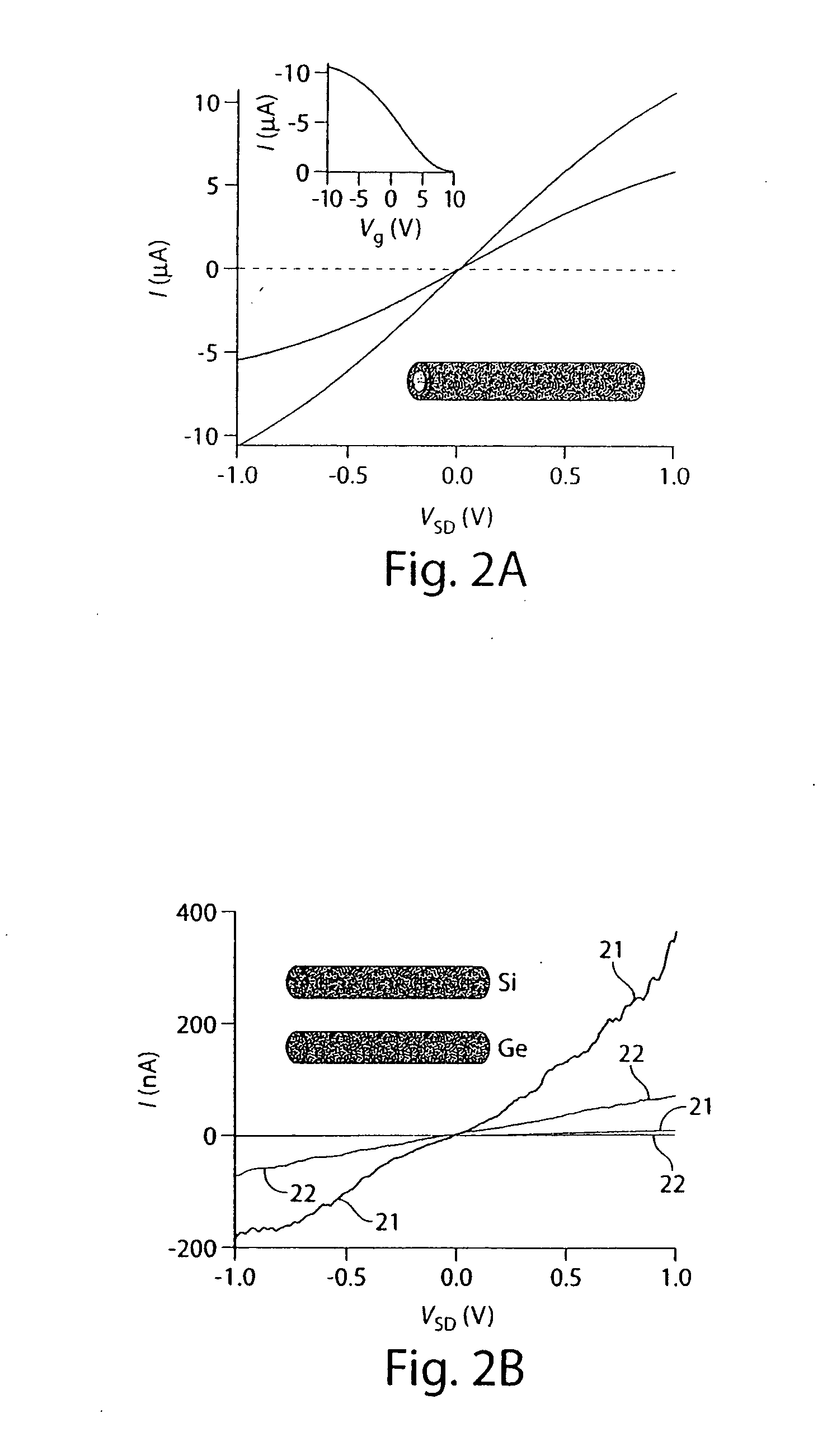
[0085]Two-dimensional electron and hole gas systems, enabled through band structure design and epitaxial growth on planar substrates, have served as key platforms for fundamental condensed matter research and high performance devices. The analogous development of one-dimensional (1D) electron or hole gas systems through controlled growth on 1D nanostructure substrates, which could open up opportunities beyond existing carbon nanotube and nanowire systems, has not been realized. This example illustrates the synthesis and transport of a 1D hole gas system based on a free-standing germanium / silicon (Ge / Si) core / shell nanowire heterostructure. Room temperature electrical transport measurements showed hole accumulation in undoped Ge / Si nanowire heterostructures, in contrast to control experiments on single component nanowires. Low-temperature studies showed controlled Coulomb blockade oscillations when the Si shell served as a tunnel barrier to the hole gas in the Ge channel. Transparent...

example 2

[0107]Silicon and germanium nanowires have been the focus of recent studies of one-dimensional (1D) FETs. However, metal contacts to single-component nanowires generally produce Schottky barriers that limit device performance, and moreover, scattering from charged dopants can also reduce the intrinsic mobility of these nanowire devices. In contrast, various aspects of the present invention show transparent contacts and low-bias ballistic transport in undoped Ge / Si core / shell nanowire heterostructures (FIGS. 7A and 7B; see also Example 1), with an estimated scattering mean free path of ˜500 nm. As will be shown in this example, the 1D sub-band spacing in the typical 15-nm core Ge / Si nanowires determined through both experimental measurements and theoretical calculations was ˜25 meV, and thus at room temperature several sub-bands may participate in NWFET transport. While the Ge / Si nanowire devices need not strictly be 1D, the limited number of conduction channels and clean material st...


PUM

PropertyMeasurementUnit
widthaaaaaaaaaa
widthaaaaaaaaaa
widthaaaaaaaaaa

Abstract

The present invention generally relates to nanoscale heterostructures and, in some cases, to nanowire heterostructures exhibiting ballistic transport, and / or to metal-semiconductor junctions that that exhibit no or reduced Schottky barriers. One aspect of the invention provides a solid nanowire having a core and a shell, both of which are essentially undoped. For example, in one embodiment, the core may consist essentially of undoped germanium and the shell may consist essentially of undoped silicon. Carriers are injected into the nanowire, which can be ballistically transported through the nanowire. In other embodiments, however, the invention is not limited to solid nanowires, and other configurations, involving other nanoscale wires, are also contemplated within the scope of the present invention. Yet another aspect of the invention provides a junction between a metal and a nanoscale wire that exhibit no or reduced Schottky barriers. As a non-limiting example, a nanoscale wire having a core and a shell may be in physical contact with a metal electrode, such that the Schottky barrier to the core is reduced or eliminated. Still other aspects of the invention are directed to electronic devices exhibiting such properties, and techniques for methods of making or using such devices.

Description

RELATED APPLICATIONS[0001]This application is a continuation-in-part of International Patent Application No. PCT / US2005 / 034345, filed Sep. 21, 2005, entitled “Nanowire Heterostructures,” by Lu, et al., published as WO 2006 / 132659 on Dec. 14, 2006, which application claims the benefit of U.S. Provisional Patent Application Ser. No. 60 / 687,807, filed Jun. 6, 2005, entitled “Nanowire Heterostructures,” by Lu, et al. Each of these applications is incorporated herein by reference.FEDERALLY SPONSORED RESEARCH[0002]Research leading to various aspects of the present invention were sponsored, at least in part, by the Defense Advanced Research Projects Agency, and the Army Research Office. The United States Government may have certain rights in the invention.FIELD OF INVENTION[0003]The present invention generally relates to nanoscale heterostructures and, in some cases, to nanowire heterostructures exhibiting ballistic transport, and / or to metal-semiconductor junctions that exhibit no or redu...

Claims


Application Information

Patent Timeline
Patent Type & Authority Applications(United States)
IPC IPC(8): H01L29/775H01L21/285H01L29/12
CPCB82Y10/00G11C2213/17G11C2213/18H01L29/165H01L29/0673H01L29/068H01L29/1606H01L29/0665
Inventor LU, WEIXIANG, JIEWU, YUETIMKO, BRIAN P.YAN, HAOLIEBER, CHARLES M.
Owner PRESIDENT & FELLOWS OF HARVARD COLLEGE
Why Eureka
Try Eureka