CLEAVED FACET (Ga,Al,In)N EDGE-EMITTING LASER DIODES GROWN ON SEMIPOLAR BULK GALLIUM NITRIDE SUBSTRATES

Active Publication Date: 2008-08-14
RGT UNIV OF CALIFORNIA
View PDF18 Cites 263 Cited by
  • Summary
  • Abstract
  • Description
  • Claims
  • Application Information

AI Technical Summary

Benefits of technology

[0016]To overcome the limitations in the prior art described above, and to overcome other limitations that will become apparent upon reading and understanding the present specification, the present invention discloses an optoelectronic device, comprising a III-nitride edge-emitting laser diode is formed on a surface of a III-nitride substrate having a semipolar ori

Problems solved by technology

The laser diodes grown on sapphire usually employ dry-etched facets which lead to higher losses and consequently to reduced efficiency.
However, such laser diodes grown hetero-epitaxially on foreign substrates (e.g., a-plane sapphire, 6H—SiC, (111) spinel, etc.) exhibit inferior performance compared to those which are grown homo-epitaxially on bulk GaN su

Method used


Image

  • CLEAVED FACET (Ga,Al,In)N EDGE-EMITTING LASER DIODES GROWN ON SEMIPOLAR BULK GALLIUM NITRIDE SUBSTRATES
  • CLEAVED FACET (Ga,Al,In)N EDGE-EMITTING LASER DIODES GROWN ON SEMIPOLAR BULK GALLIUM NITRIDE SUBSTRATES
  • CLEAVED FACET (Ga,Al,In)N EDGE-EMITTING LASER DIODES GROWN ON SEMIPOLAR BULK GALLIUM NITRIDE SUBSTRATES

Examples


Embodiment Construction

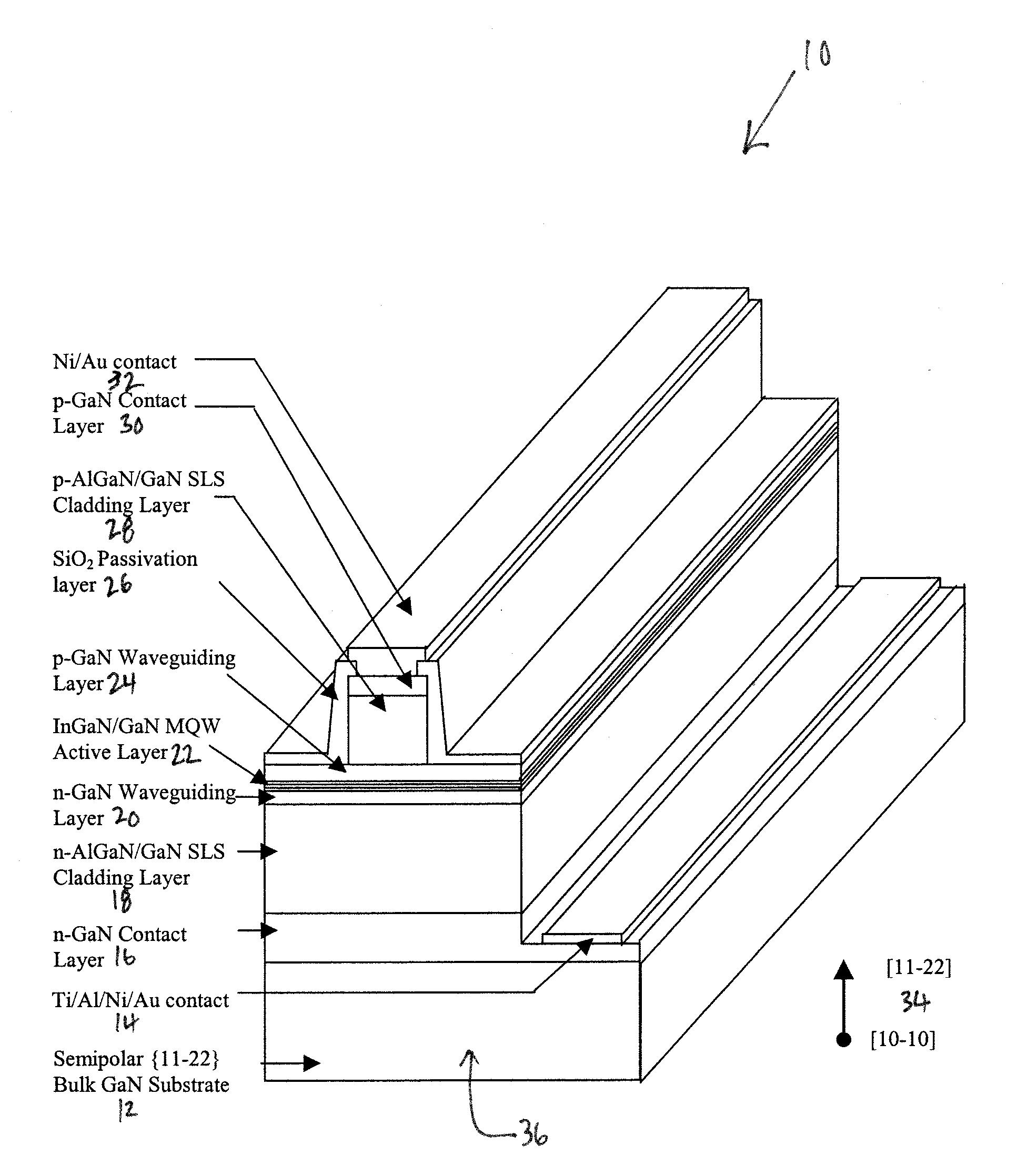
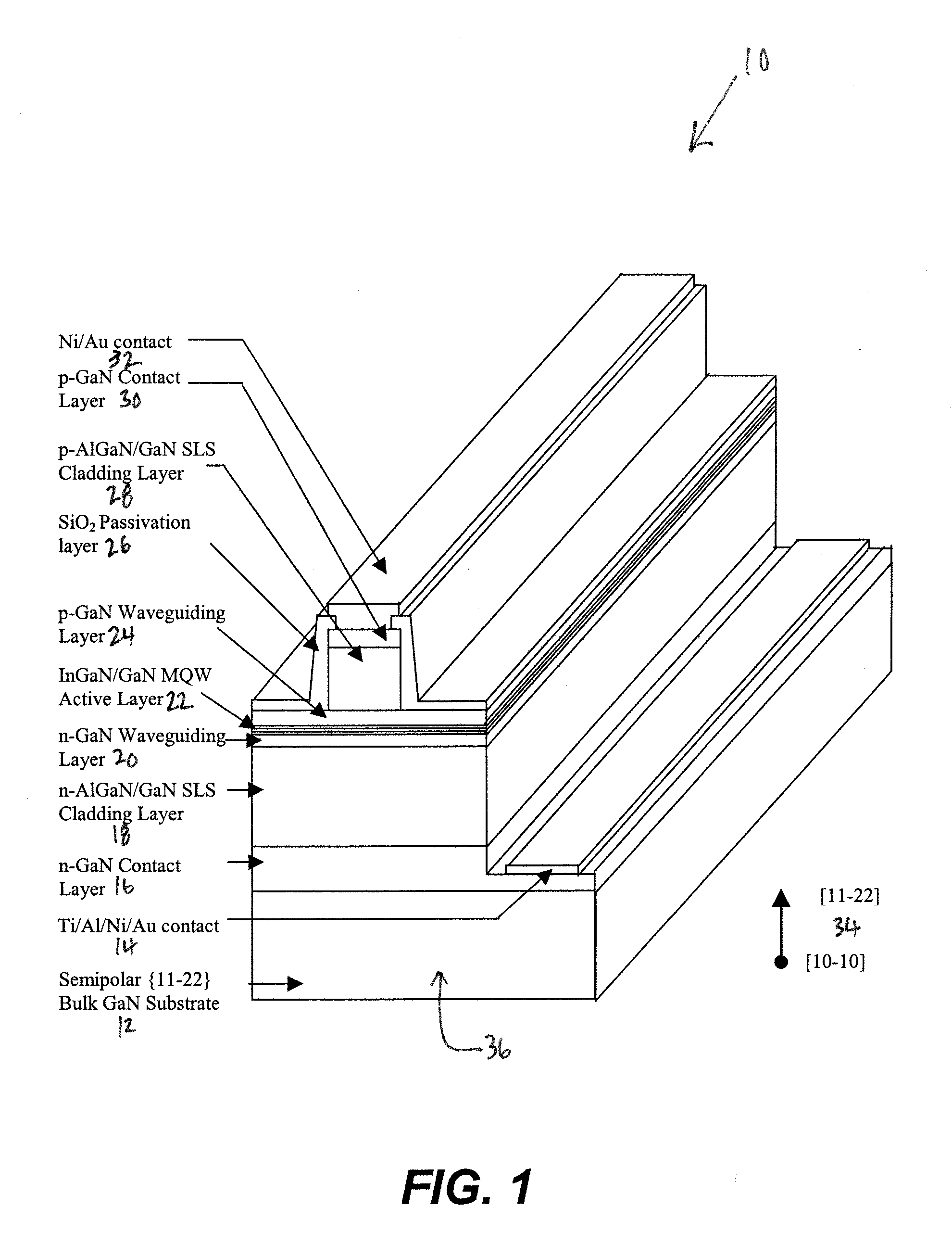
[0021]In the following description of the preferred embodiment, reference is made to the accompanying drawings that form a part hereof, and in which is shown by way of illustration a specific embodiment in which the invention may be practiced. It is to be understood that other embodiments may be utilized and structural changes may be made without departing from the scope of the present invention.

[0022]The present invention discloses a III-nitride semiconductor light emitting device formed on a surface of a III-nitride substrate having a semipolar orientation, for example, an edge-emitting laser diode, comprised of semiconductor material alloys (Ga,In,Al)N, namely Group-III nitride layers (also known as III-nitride layers), such as gallium-containing, indium-containing, and / or aluminum-containing nitride layers. The device is fabricated using well-established semiconductor device processing techniques.

[0023]FIG. 1 is a detailed schematic of one embodiment of the device of the present...


PUM


Abstract

A III-nitride edge-emitting laser diode is formed on a surface of a III-nitride substrate having a semipolar orientation, wherein the III-nitride substrate is cleaved by creating a cleavage line along a direction substantially perpendicular to a nonpolar orientation of the III-nitride substrate, and then applying force along the cleavage line to create one or more cleaved facets of the III-nitride substrate, wherein the cleaved facets have an m-plane or a-plane orientation.

Description

CROSS-REFERENCE TO RELATED APPLICATION[0001]This application claims the benefit under 35 U.S.C. Section 119(e) of the following co-pending and commonly-assigned U.S. patent application:[0002]U.S. Provisional Application Ser. No. 60 / 889,518, filed on Feb. 12, 2007, by Shuji Nakamura, James S. Speck, Steven P. DenBaars, and Anurag Tyagi, entitled “CLEAVED FACET (Ga,Al,In)N EDGE-EMITTING LASER DIODES GROWN ON SEMIPOLAR {11-2n} BULK GaN SUBSTRATES,” attorneys' docket number 30794.221-US-P1 (2007-423-1);[0003]which application is incorporated by reference herein.BACKGROUND OF THE INVENTION[0004]1. Field of the Invention[0005]The present invention is related to a semiconductor optical device based on a semipolar substrate.[0006]2. Description of the Related Art[0007](Note: This application references a number of different publications as indicated throughout the specification by one or more reference numbers within parentheses, e.g., (Ref. X). A list of these different publications ordere...

Claims


Application Information

Patent Timeline
IPC IPC(8): H01L33/00H01L21/00
CPCB82Y20/00H01S5/0202H01S5/34333H01S5/2201H01S5/3216H01S5/22
Inventor NAKAMURA, SHUJISPECK, JAMES S.DENBAARS, STEVEN P.TYAGI, ANURAG
Owner RGT UNIV OF CALIFORNIA
Why Eureka
Try Eureka