Chip package structure and method of fabricating the same

a chip and package technology, applied in the direction of solid-state devices, basic electric elements, electric devices, etc., can solve the problems of increasing the additional manufacturing cost of the lead frame, the mask required in the photolithography process of patterning the lead frame, etc., to save the production cost of the chip package structure and reduce packaging costs

Inactive Publication Date: 2008-08-14
CHIPMOS TECH INC
View PDF2 Cites 23 Cited by
  • Summary
  • Abstract
  • Description
  • Claims
  • Application Information

AI Technical Summary

Benefits of technology

[0011]The present invention is directed to a chip package structure and a method of fabricating the same, so as to reduce the packaging costs arisen from directly employing patterned lead frames in a conventional chip packaging process. Specifically, a metal thin plate is used in the present invention, and a die pad, a bus bar and leads of the lead frame are formed on the metal thin plate through performing an etching step during the packaging process, which is helpful to save the production costs of the chip package structure.

Problems solved by technology

However, masks required in the photolithography process of patterning the lead frame are rather expensive, thereby increasing additional manufacturing costs of the lead frame.

Method used


Image

  • Chip package structure and method of fabricating the same
  • Chip package structure and method of fabricating the same
  • Chip package structure and method of fabricating the same

Examples


second embodiment

[0053]FIG. 6 is a schematic cross-sectional view of a chip package structure according to a second embodiment of the present invention. It should be noted that the same or similar reference numbers used in the second embodiment and in the first embodiment represent the same or the like elements, and the second embodiment is approximately identical to the first embodiment. The difference between the two embodiments will be described hereinafter, and the similarities therebetween are omitted.

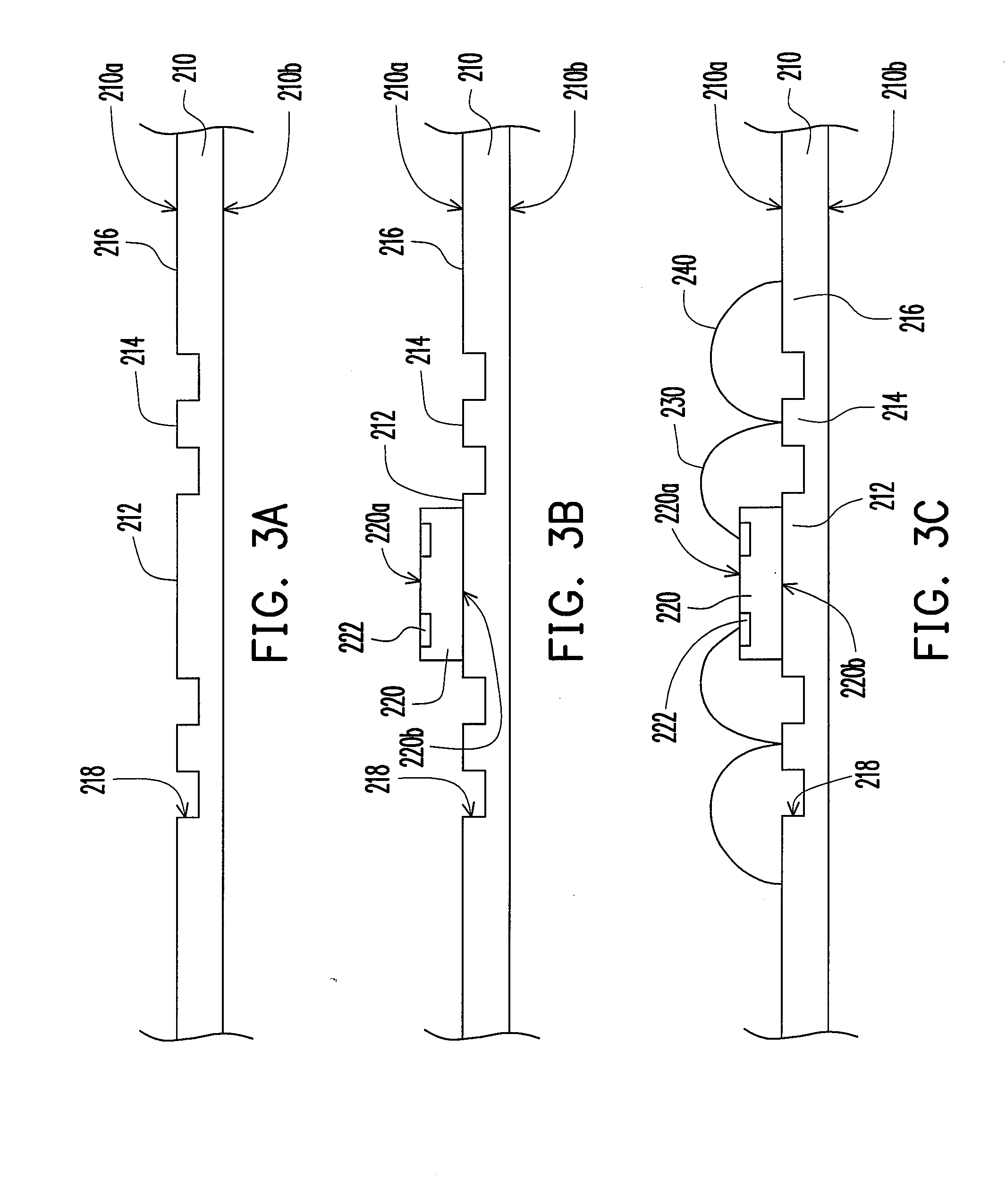
[0054]Referring to FIG. 6, the difference between the second embodiment and the first embodiment lies in that a second protrusion part 514 of a metal thin plate 510 has a down-set design in a chip package structure 500. That is to say, an upper surface 510a of the second protrusion part 514 is lower than the upper surface 510a of a first protrusion part 212 and the upper surface 510a of a plurality of third protrusion parts 216. After a lead frame 510′ of the metal thin plate 510 is formed, and th...

third embodiment

[0055]FIG. 7 is a schematic cross-sectional view of a chip package structure according to a third embodiment of the present invention. It should be noted that the same or similar reference numbers used in the third embodiment and in the first embodiment represent the same or the like elements, and the third embodiment is approximately identical to the first embodiment. The difference between the two embodiments is described hereinafter, and the similarities therebetween are omitted.

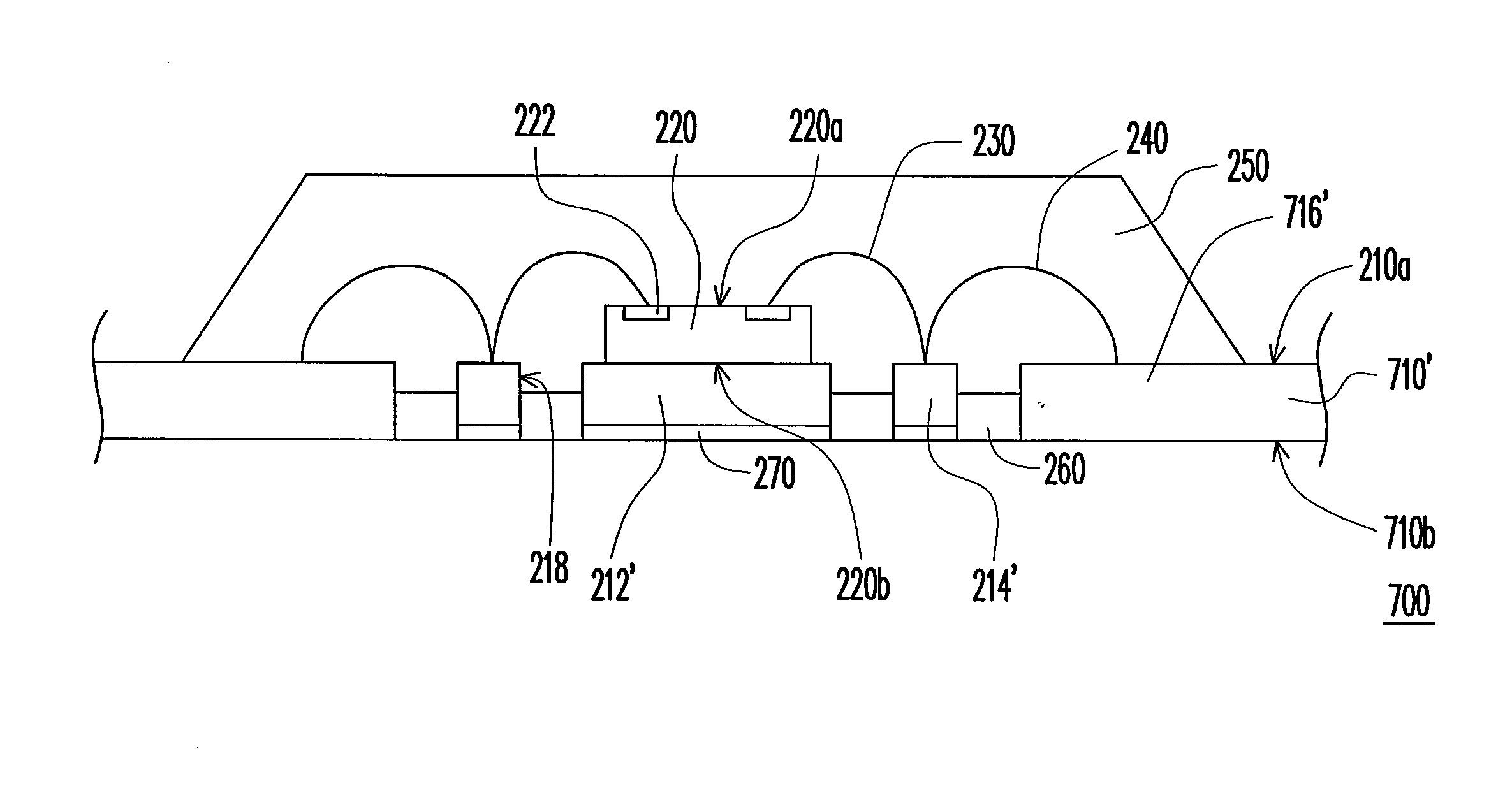
[0056]Please refer to FIG. 7. The difference between the third embodiment and the first embodiment lies in that a thickness of a die pad 612′ exceeds the thicknesses of a bus bar 214′ and of a plurality of leads 216′ in a lead frame 610′ of a chip package structure 600. And an upper surface 210a of the die pad 612′ is coplanar with the upper surface 210a of the bus bar 214′ and the upper surface 210a of the leads 216′. After the fabrication of the chip package structure 600 is basically completed, an etch...


PUM


Abstract

A method of fabricating a chip package structure includes the steps of providing a metal thin plate having a first protrusion part, a second protrusion part and a plurality of third protrusion parts. A chip is then disposed on the metal thin plate and a plurality of bonding wires is formed to electrically connect the chip to the second protrusion part and connect the second protrusion part to the third protrusion parts. Next, an upper encapsulant and a lower encapsulant are formed on an upper surface and a lower surface of the metal thin plate, respectively. Thereafter, an etching mask is formed on the lower surface and exposes the connections among the protrusion parts. Finally, the metal thin plate is etched, such that the first protrusion part, the second protrusion part and the third protrusion parts form a die pad, a bus bar and leads of a lead frame, respectively.

Description

CROSS-REFERENCE TO RELATED APPLICATION[0001]This application claims the priority benefit of P.R.C. application serial no. 200710005145.0, filed Feb. 8, 2007. All disclosure of the P.R.C. application is incorporated herein by reference.BACKGROUND OF THE INVENTION[0002]1. Field of the Invention[0003]The present invention relates to a chip package structure. More particularly, the present invention relates to a chip package structure with a lead frame.[0004]2. Description of Related Art[0005]The production of integrated circuit (IC) devices is mainly divided into three stages including IC design, IC process and IC package.[0006]During the IC process, a chip is manufactured by the steps of wafer fabrication, IC formation, wafer sawing and so on. A wafer has an active surface, which generally refers to the surface including active devices. After the IC inside the wafer is completely formed, a plurality of bonding pads is further disposed on the active surface of the wafer, such that the ...

Claims


Application Information

Patent Timeline
Patent Type & Authority Applications(United States)
IPC IPC(8): H01L23/495H01L21/60
CPCH01L21/4828H01L23/3107H01L2924/014H01L2924/01087H01L2924/01006H01L2924/00014H01L2924/3025H01L2924/19107H01L23/495H01L24/48H01L24/49H01L24/85H01L2221/68377H01L2224/48091H01L2224/48247H01L2224/4911H01L2224/85001H01L2924/01005H01L2924/01015H01L2924/01029H01L2924/01082H01L2924/14H01L2224/78H01L2224/05554H01L2924/10161H01L2924/181H01L2224/45099H01L2224/05599H01L2924/00012
Inventor QIAO, YONG-CHAOWU, YAN-YICHIOU, JIE-HUNG
Owner CHIPMOS TECH INC
Why Eureka
Try Eureka