
Eureka
For R&D, Eureka makes reading and utilizing patents & technical documents easy.
Eureka AIR
Designed for self-driven R&D workflows. Generate viable solutions, solve complex R&D challenges, empower your innovation with AI.

Eureka Materials
Designed for material experts only. Revolutionize your material R&D, from search, analyze, to developing new materials.

TechResearch
Generate reliable direction feasibility study reports for your R&D in just a few steps.

TechSeek
Discover and master advanced knowledge NOW. Basics, ideas, possibilities, all at once.

TechMind
As an expert in R&D Theories, TechMind can generates customized viable solutions instantly.

TechRisk
Analyze your overall solution with one click, know your potential R&D risks in advance.

TechMonitor
Get weekly tech updates, stay abreast of the latest tech innovations and key insights.
Method of fabricating micro connectors
- Summary
- Abstract
- Description
- Claims
- Application Information
AI Technical Summary
Benefits of technology
Problems solved by technology
Method used
Image

Examples
Embodiment Construction
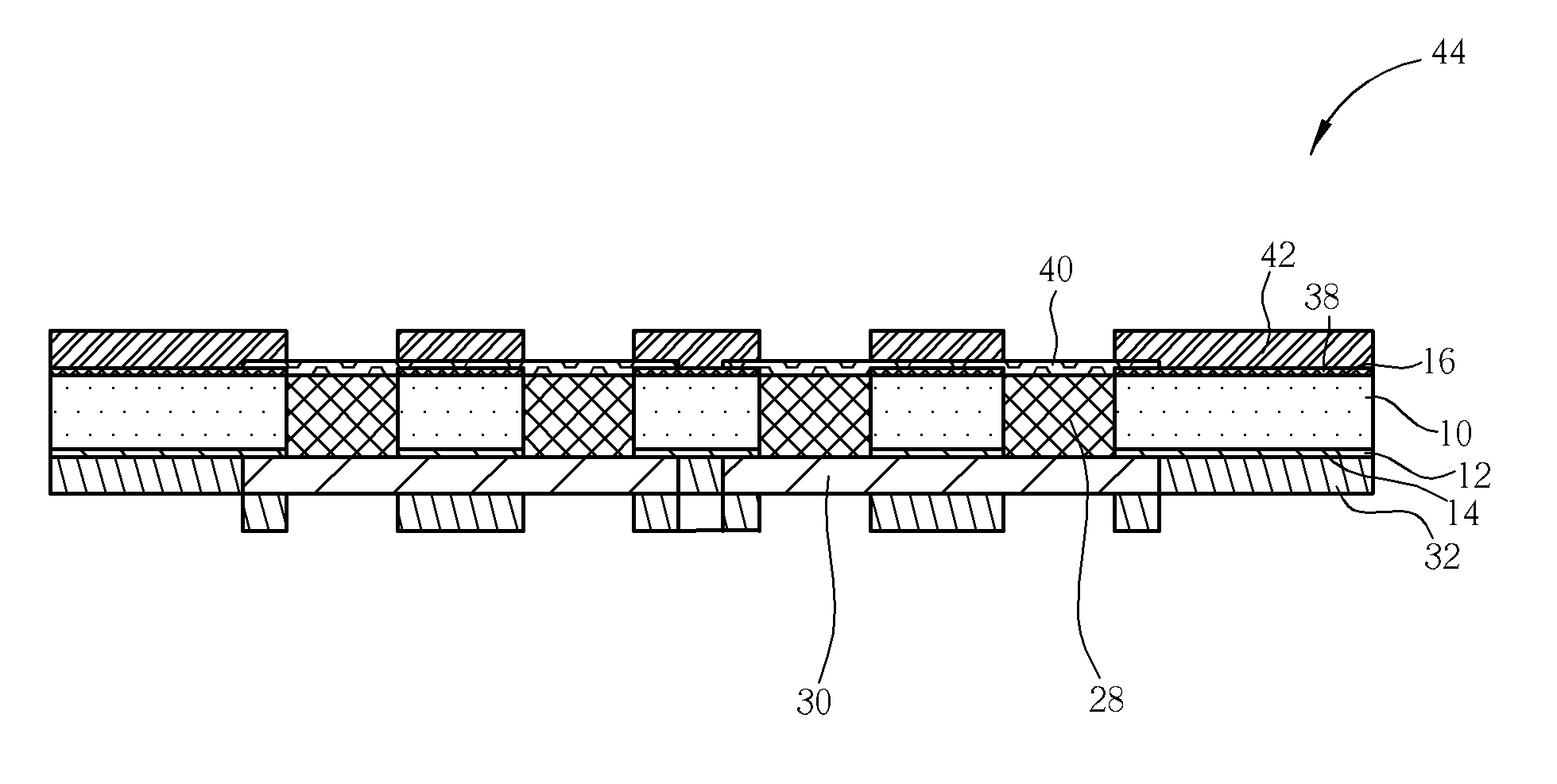
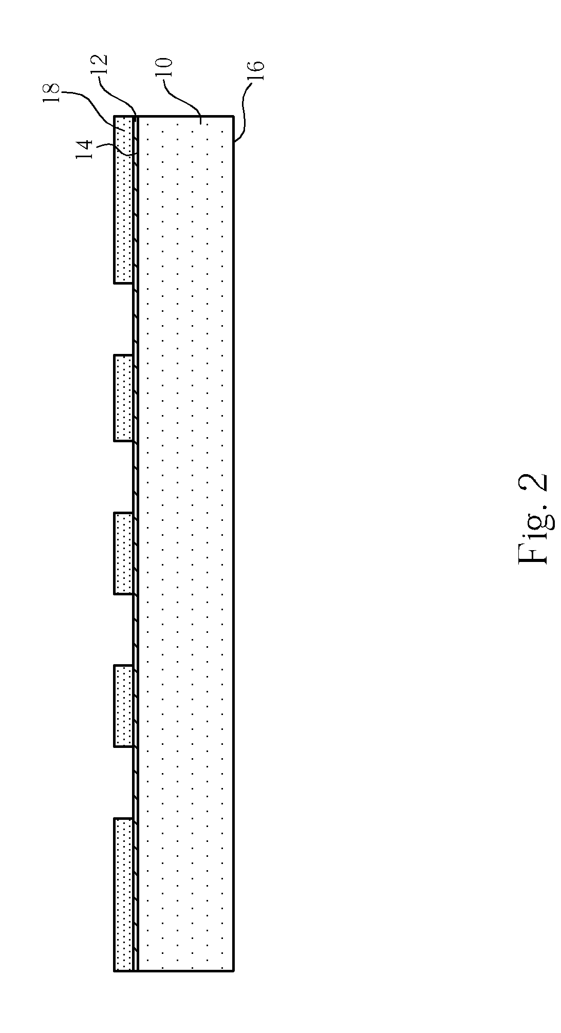
[0012]Please refer to FIG. 1 through FIG. 17. FIG. 1 through FIG. 17 are schematic diagrams illustrating a method of fabricating micro connectors according to a preferred embodiment of the present invention. As shown in FIG. 1, first, a wafer 10, such as a silicon wafer, is provided, and the wafer 10 includes a first surface 14 and a second surface 16. Then, a first dielectric layer 12 is formed on the first surface 14 of the wafer 10. In this embodiment, the first dielectric layer 12 is an oxide layer formed by a thermal deposition, and the function of the first dielectric layer 12 provides insulation to avoid leakage current. The forming method and material of the first dielectric layer 12 are not limited to the above-mentioned, and the first dielectric layer 12 can be another insulating material, such as silicon oxide, silicon nitride or silicon oxy-nitride.
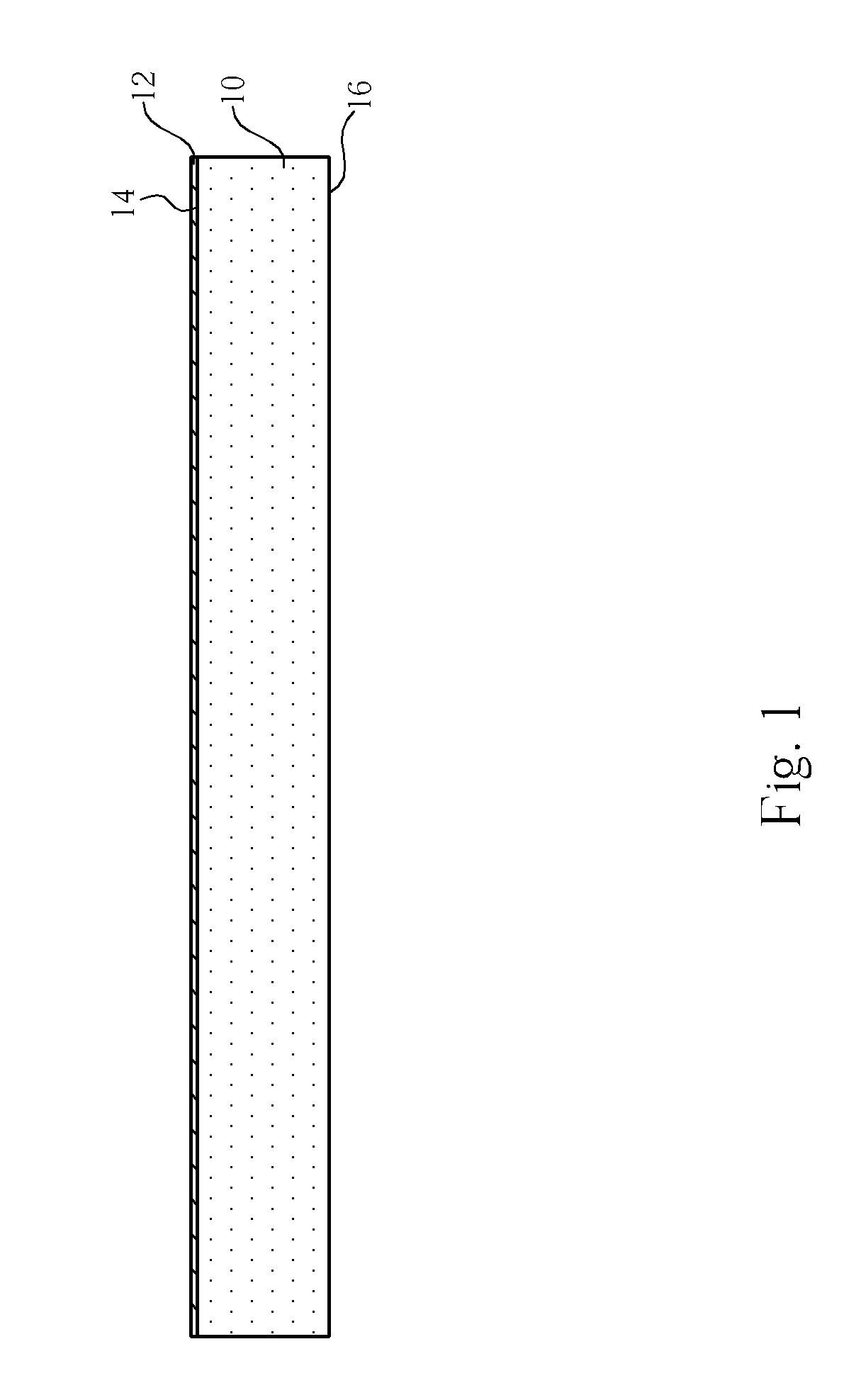
[0013]Next, as shown in FIG. 2, a mask pattern 18 is formed on the first dielectric layer 12. The mask pattern 18 can be a p...
PUM
 Abstract
Description
Claims
Application Information
 - R&D Engineer
- R&D Manager
- IP Professional
- Industry Leading Data Capabilities
- Powerful AI technology
- Patent DNA Extraction
Browse by: Latest US Patents, China's latest patents, Technical Efficacy Thesaurus, Application Domain, Technology Topic, Popular Technical Reports.
© 2024 PatSnap. All rights reserved.Legal|Privacy policy|Modern Slavery Act Transparency Statement|Sitemap|About US| Contact US: help@patsnap.com