Group ii alloyed i-iii-vi semiconductor nanocrystal compositions and methods of making same

a semiconductor nanocrystal and composition technology, applied in the field of group ii alloyed iiiivi semiconductor nanocrystal compositions, can solve the problems of reducing quantum yield, little work on i-iii-vi semiconductor nanocrystals, and materials produced via these methods are not useful for applications where fluorescence is important, and achieve high luminescent quantum yield

Inactive Publication Date: 2008-08-28
EVIDENT TECH
View PDF1 Cites 64 Cited by
  • Summary
  • Abstract
  • Description
  • Claims
  • Application Information

AI Technical Summary

Benefits of technology

[0015]In an embodiment, the present invention provides a semiconductor nanocrystal composition comprising a group II element alloyed with a I-III-VI semiconductor nanocrystal core, wherein the semiconductor nanocrystal composition is stable and exhibits a high luminescent quantum yield.
[0016]In another embodiment, the present invention provides a method of making a semiconductor nanocrystal composition comprising a group II element and alloyed to I-III-VI semiconductor nanocrystal core, wherein the semiconductor nanocrystal composition is stable and exhibits a high luminescent quantum yield.

Problems solved by technology

Because the nanocrystal may have a large surface area to volume ratio, dislocations present on the surface or adsorbed surface molecules having a significant potential difference from the nanocrystal itself will tend to trap excited state carriers and prevent radiative recombination and thus reduce quantum yield.
As a result semiconductor nanocrystals, which do not include these elements are desired for many quantum dot applications such as light emitting diodes, visual displays, solar cells (photovoltaic cells).
Although much work has been done using visible to near infrared emitting III-V nanocrystal materials, such as InP and InGaP, very little work has been done on I-III-VI semiconductor nanocrystals.
Also reported in the Nakamura paper is the use of a mercaptounadecanoinc acid as a ligand to render them water soluble, however due to the low reported quantum yields the materials produced via these methods are not useful for applications where fluorescence is important.

Method used


Image

  • Group ii alloyed i-iii-vi semiconductor nanocrystal compositions and methods of making same
  • Group ii alloyed i-iii-vi semiconductor nanocrystal compositions and methods of making same
  • Group ii alloyed i-iii-vi semiconductor nanocrystal compositions and methods of making same

Examples


example

Preparing a Group II Alloyed I-III-VI Semiconductor Nanocrystal Composition

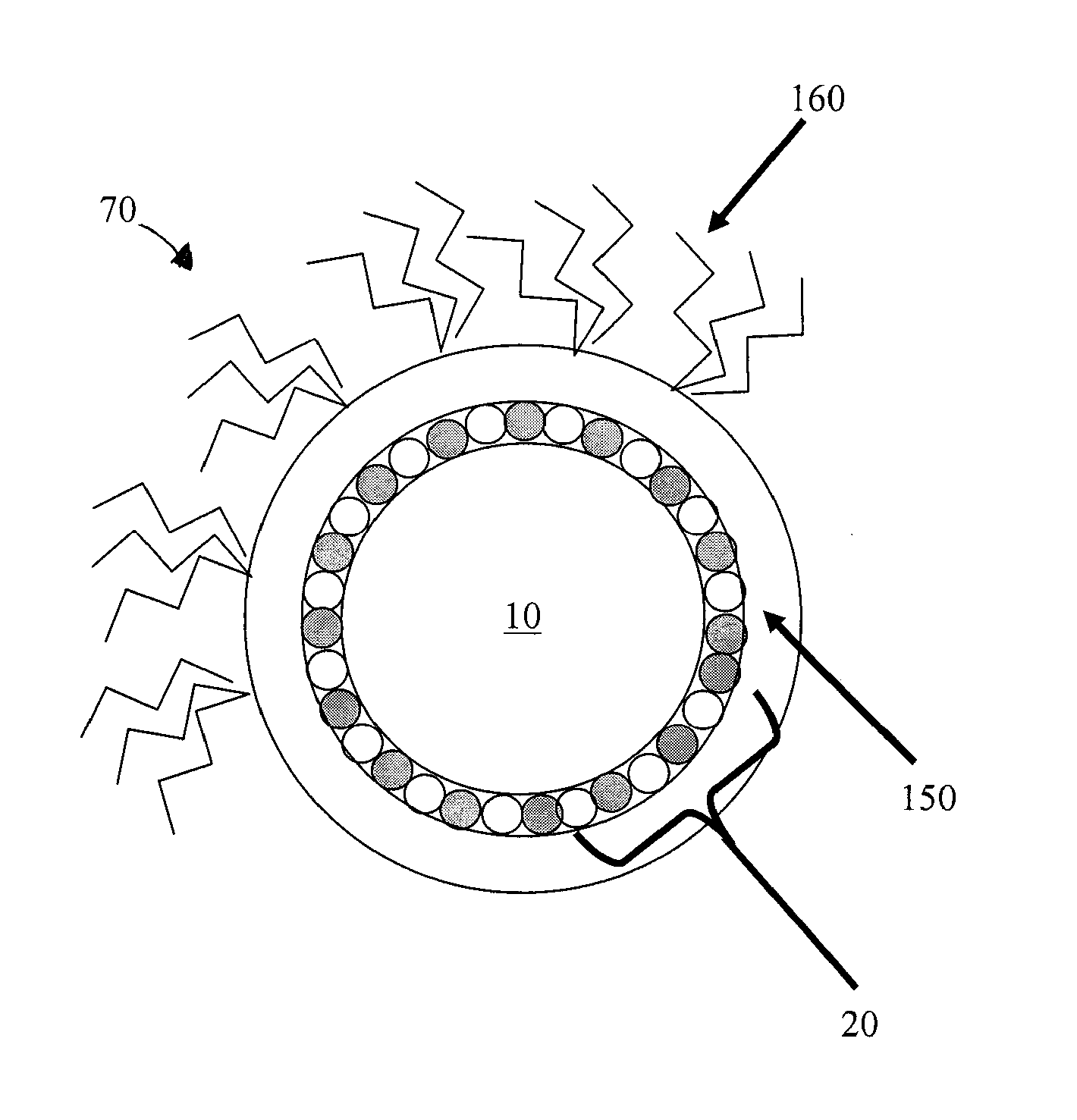
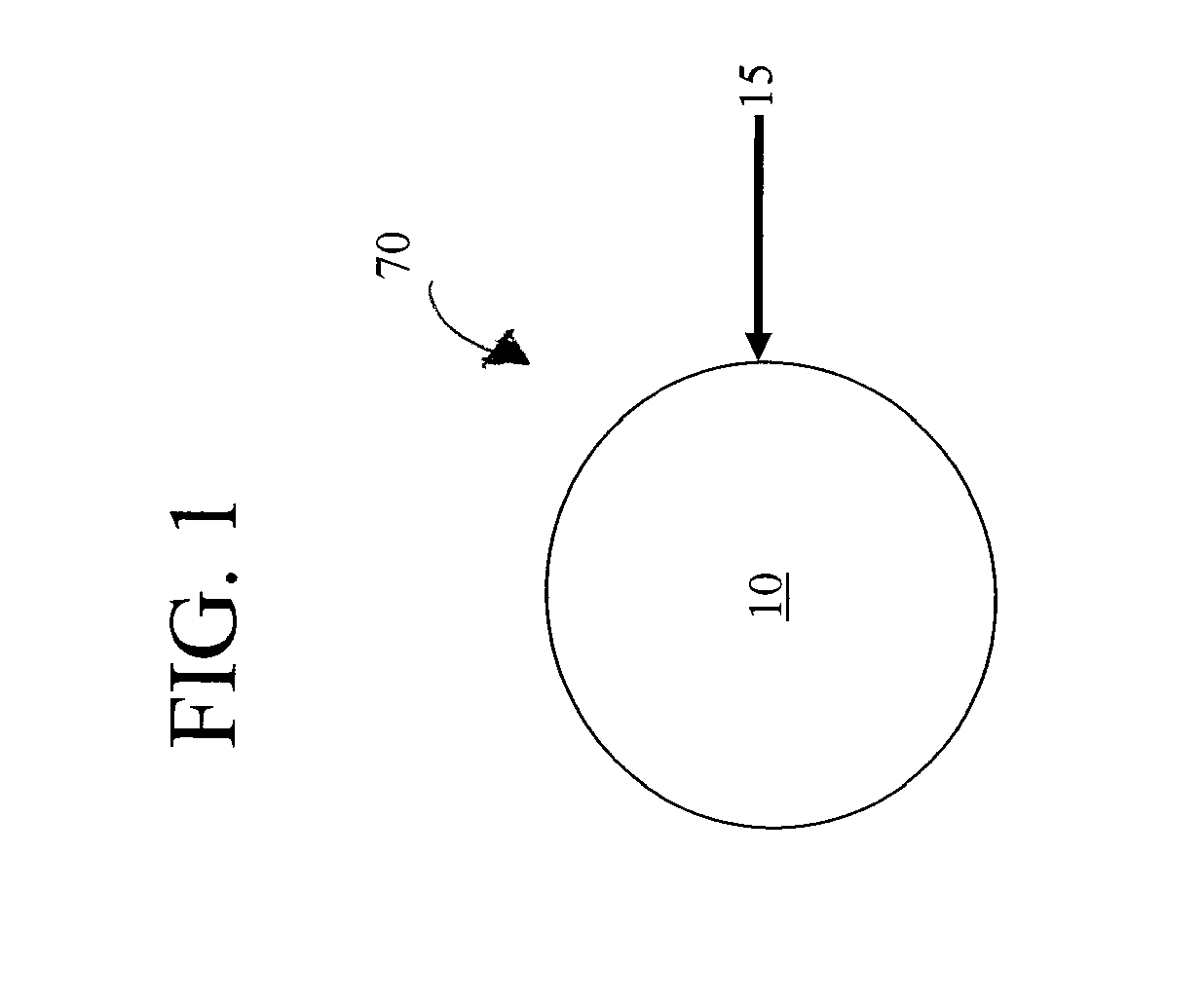
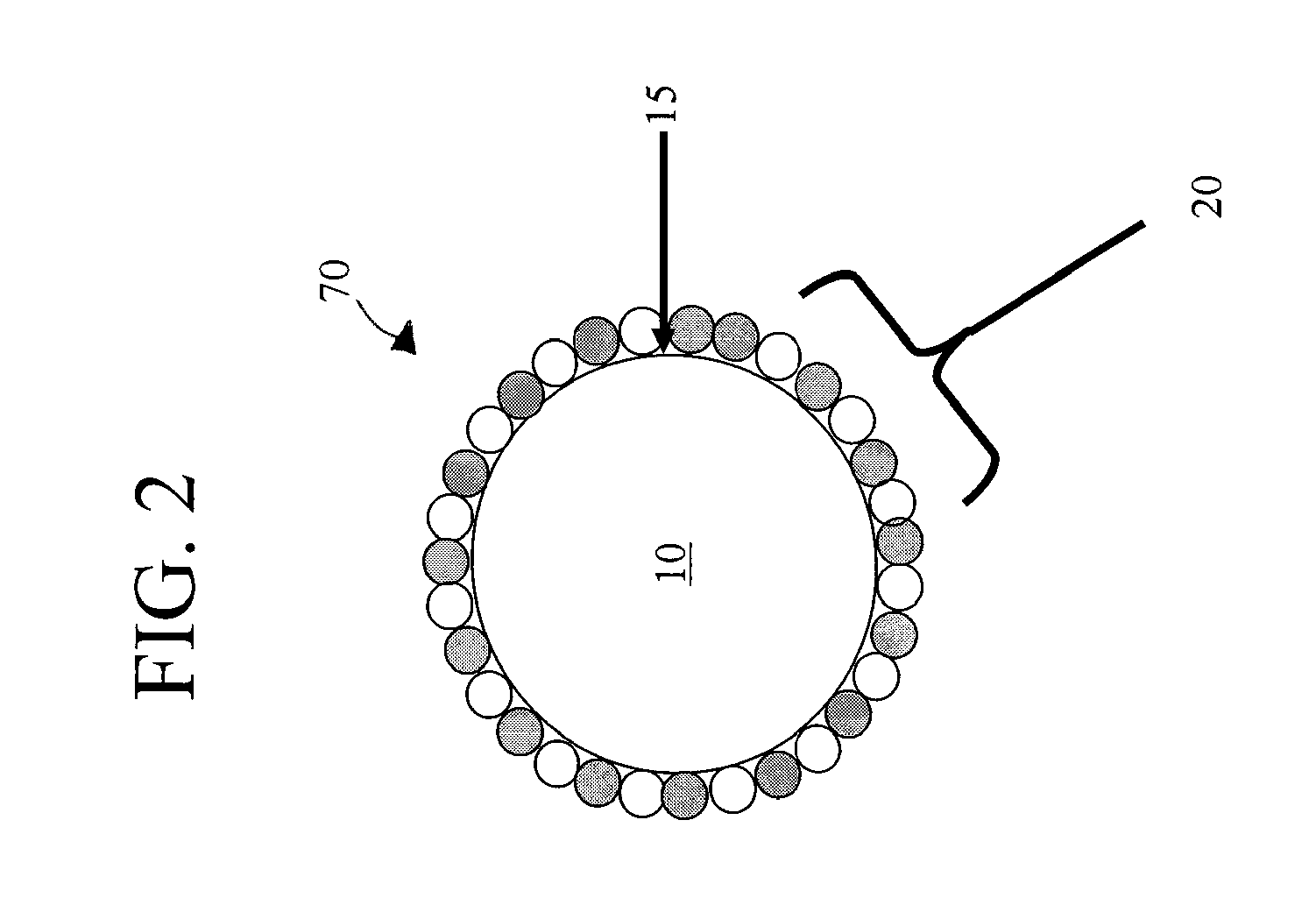
[0047]The present example discloses how to prepare a stable, high luminescent quantum yield semiconductor nanocrystal composition comprising a core of ZnCuInGaS2, a Zn metal layer formed on the outer surface of the semiconductor nanocrystal core after synthesis of the core, and a ZnS shell formed on the Zn metal layer. However, the teachings of the below procedure may be used to produce other group II alloyed I-III-VI nanocrystal compositions discussed above.

[0048]The first step is preparing an indium and gallium precursor. In a reaction flask, 292 g / mol of 0.9 Molar indium (III) acetate (99.99% pure) is added to 367 g / mol of 0.1 Molar gallium acetylacetonate (99% pure) and 256.4 g / mol of 3 Molar palmitic acid (99% pure). The ingredients are mixed and heated to 130° C. for 2 hours under vacuum. The vacuum removes any acetic acid that could form. The resulting precursor solution should be clear but may have a ...


PUM

PropertyMeasurementUnit
peak emission wavelengthaaaaaaaaaa
diameteraaaaaaaaaa
diameteraaaaaaaaaa

Abstract

A semiconductor nanocrystal composition that is stable and has high luminescent quantum yield. The semiconductor nanocrystal composition has a semiconductor nanocrystal core of a group II alloyed I-III-VI semiconductor nanocrystal material. A method of making a semiconductor nanocrystal composition is also provides which includes synthesizing a semiconductor nanocrystal core of a group II alloyed I-III-VI semiconductor material.

Description

CROSS REFERENCE TO RELATED APPLICATIONS[0001]The present application claims priority to U.S. Provisional Patent Application No. ______, entitled “Group II Alloyed I-III-VI Semiconductor Nanocrystal Compositions and Methods of Making the Same,” filed Jan. 24, 2007, which is incorporated by reference herein.FIELD OF THE INVENTION[0002]The present invention relates to semiconductor nanocrystal compositions and particularly to group II alloyed I-III-VI semiconductor nanocrystal compositions. The present invention also relates to methods of making semiconductor nanocrystal compositions.BACKGROUND OF THE INVENTION[0003]Semiconductor nanocrystals are typically crystals of II-VI, III-V, IV-VI materials that have a diameter between 1 nanometer (nm) and 20 nm. More recently other semiconductor nanocrystals made from ternary semiconductors such as I-III-VI semiconductors have been disclosed. In the strong confinement limit, the physical diameter of the nanocrystal is smaller than the bulk exci...

Claims


Application Information

Patent Timeline
Patent Type & Authority Applications(United States)
IPC IPC(8): C09D1/00
CPCB82Y20/00B82Y30/00C01B19/002C01B19/007C01G15/006C01P2002/84C01P2004/84C01P2004/80C01P2006/40H01L21/02568H01L21/02601C01G9/06C01P2002/82C01P2004/64
Inventor SHI, WEILI
Owner EVIDENT TECH
Why Eureka
Try Eureka