Charged Particle Beam Apparatus

a particle beam and apparatus technology, applied in the direction of material analysis using wave/particle radiation, instruments, nuclear engineering, etc., can solve the problems of difficult control, affecting the operability of the probe significantly affecting the operation precision and efficiency, etc., to facilitate the operation of precise probe contact.

Inactive Publication Date: 2008-08-28
HITACHI HIGH-TECH CORP
View PDF1 Cites 36 Cited by
  • Summary
  • Abstract
  • Description
  • Claims
  • Application Information

AI Technical Summary

Benefits of technology

[0008]The present invention has as its object to improve contact precision and probe operability.
[0014]Preferably, a shape of the tip of the probe which has been deformed is shaped by precisely arranging the tip of the probe within an observation area and applying a charged particle beam to an area of a regular shape.
[0019]The present invention facilitates precise probe contact operation to a sample position of the order of microns.

Problems solved by technology

Although movement of a sample stage by precise drive control is also important, it is not easy to always control to move the sample stage to a desired position, even allowing for the tolerance of a connection position of a micro-sample.
Conventional micro-sampling is work in a minute space, and the operability of a probe significantly affects operating precision and efficiency.
Additionally, a heavy burden is placed on an operator due to the importance of a sample, the durability of a probe itself, and the like.

Method used


Image

  • Charged Particle Beam Apparatus
  • Charged Particle Beam Apparatus
  • Charged Particle Beam Apparatus

Examples


Embodiment Construction

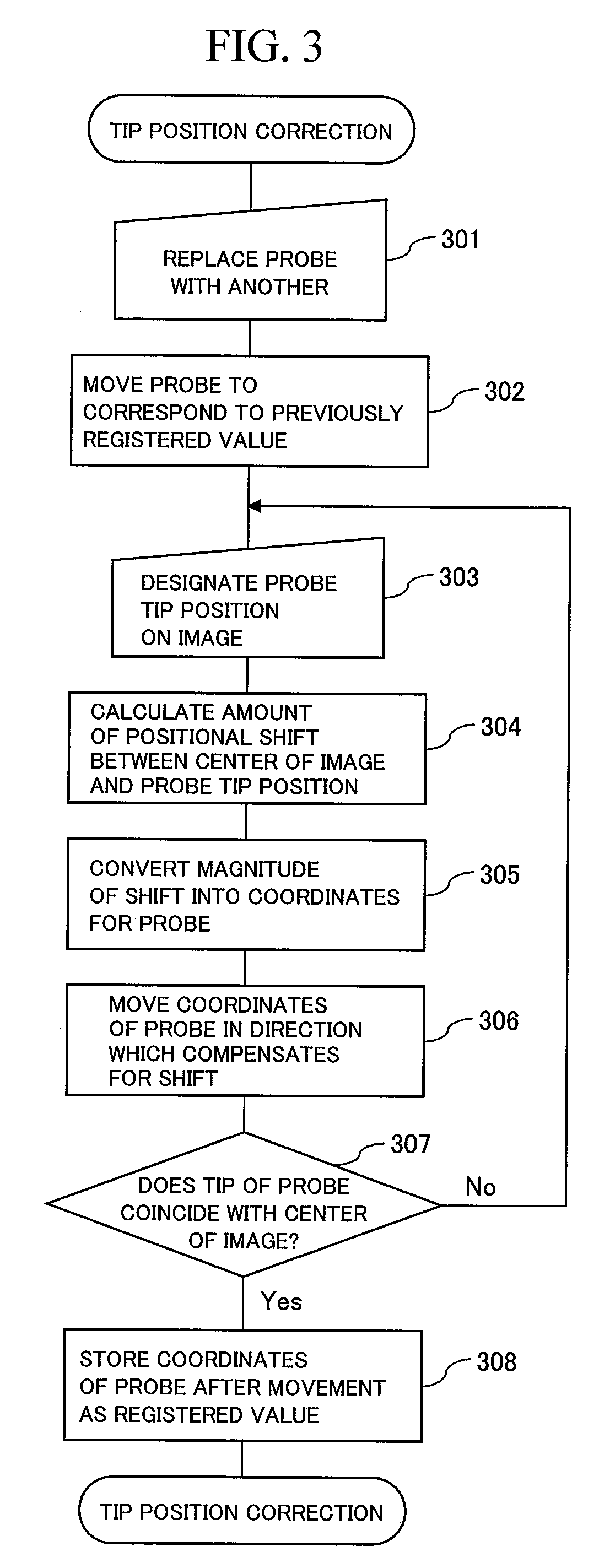
[0030]The foregoing and other novel features and advantages of the present invention will be described below with reference to the drawings. Note that the drawings are illustrative only and not intended to restrict the scope of right.

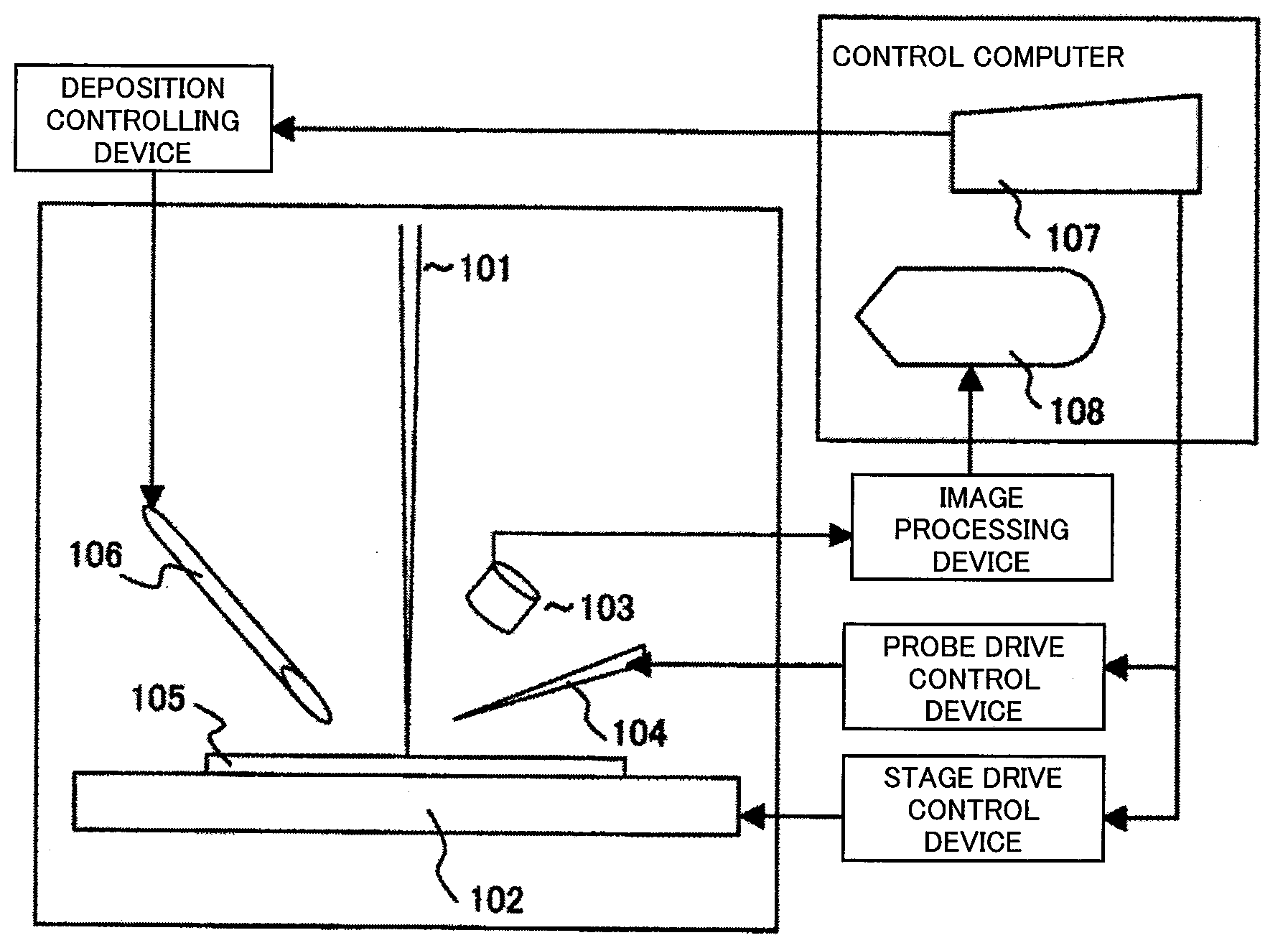
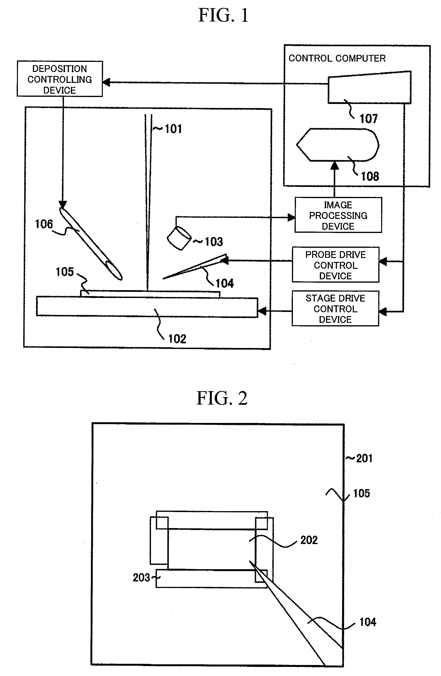
[0031]FIG. 1 is a schematic view of a charged particle beam processing and observation apparatus having a probe drive control mechanism and represents a unit pertaining to this embodiment of a mechanism constituting the processing and observation apparatus.

[0032]The apparatus includes a charged particle beam generating section, a charged particle beam irradiating optical system section, a stage on which a sample is mounted and which can move below a charged particle beam, a control section which drives the stage, an electron detecting section which detects a particle emitted from the sample, a control section which acquires an observation image by synchronizing a detection signal from the electron detecting section and charged particle beam scanning, a ...


PUM

PropertyMeasurementUnit
shapeaaaaaaaaaa
areaaaaaaaaaaa
heightsaaaaaaaaaa

Abstract

It is an object of this invention to improve contact precision and probe operability. This invention controls sample stage movement and probe movement on an observation image using a single coordinate system, thereby allowing positioning using a sample stage stop error as a probe control movement amount. This invention also figures out the position of the tip of a probe using the observation image and stores the coordinates of the probe at a reference position on the image. This invention facilitates precise probe contact operation to a sample position of the order of microns.

Description

BACKGROUND OF THE INVENTION[0001]1. Field of the Invention[0002]The present invention relates to a technique for extracting a piece of a sample including a desired area from a semiconductor wafer, a semiconductor device, or the like using ion beams.[0003]2. Background Art[0004]Manufacture of semiconductor devices such as a semiconductor memory and a microprocessor and electronic components such as a magnetic head requires characteristic inspection for product quality control. The characteristic inspection includes measurement of manufacturing dimension, inspection of a circuit pattern for a defect, and analysis of foreign bodies. Various means are prepared to perform these inspections. If an abnormality is found inside a product, a micromachining and observation apparatus using a focused ion beam (FIB) is used. This apparatus includes a function of cutting out a minute area of the order of microns including an observation part and producing a minute sample for facilitating observati...

Claims


Application Information

Patent Timeline
Patent Type & Authority Applications(United States)
IPC IPC(8): G01N23/225G21K5/10
CPCG01N23/225H01J37/3045H01J2237/31745H01J2237/024H01J2237/221H01J37/3056
Inventor KOZUMA, TOSHIAKIYOSHIZAWA, YUKIOAIZAWA, MEGUMI
Owner HITACHI HIGH-TECH CORP
Why Eureka
Try Eureka