
Nonvolatile RAM

Inactive Publication Date: 2008-08-28
LONGITUDE SEMICON S A R L
View PDF6 Cites 21 Cited by
  • Summary
  • Abstract
  • Description
  • Claims
  • Application Information

AI Technical Summary

Benefits of technology

[0030]As described above, the present invention offers the following effects.
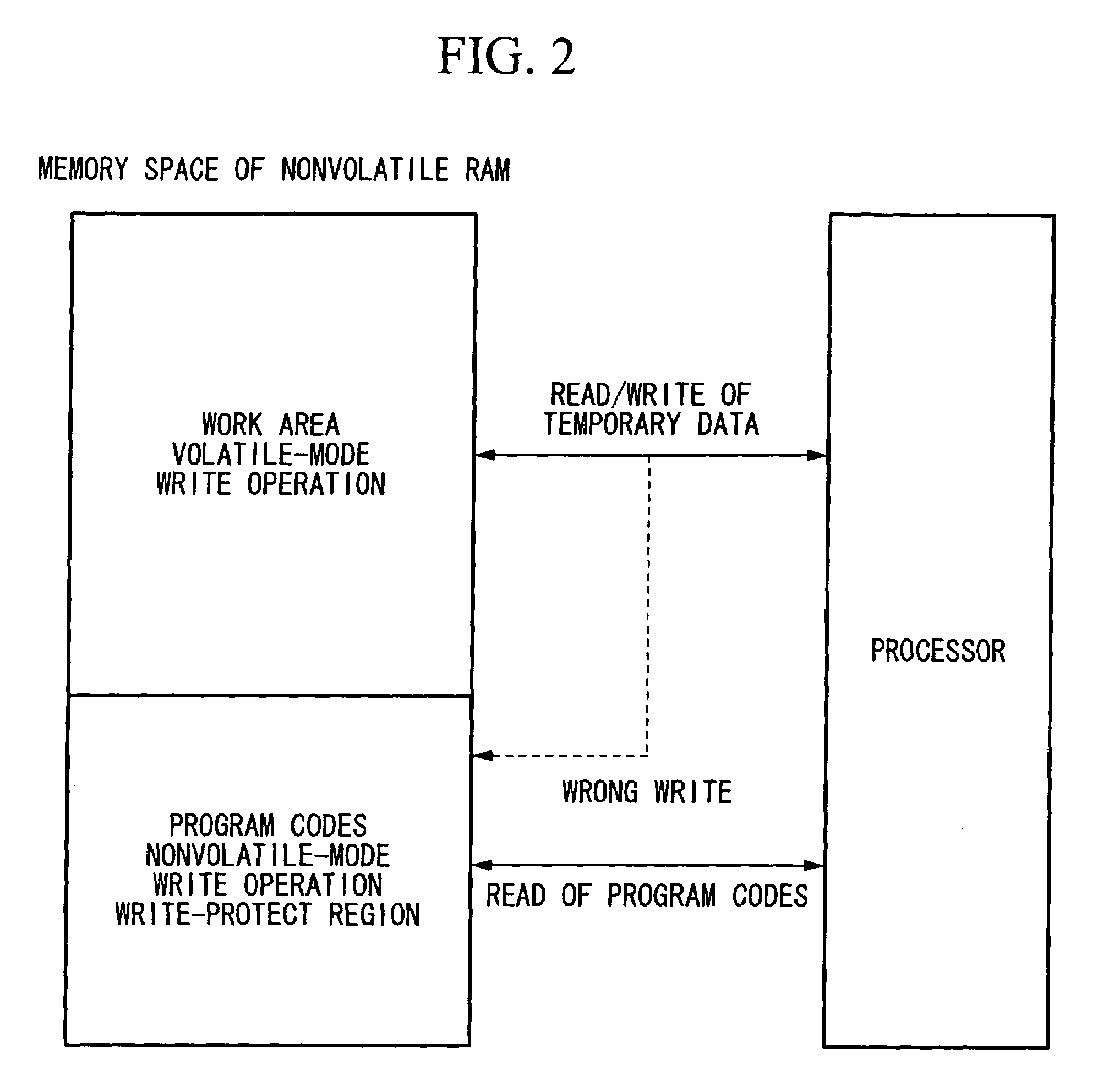
[0031]The aforementioned nonvolatile RAM is designed to store fixed data such as program codes and table data, which are not necessarily changed, in the first portion of the memory area subjected to the nonvolatile-mode write operation while using the second portion of the memory area (serving as the work area) subjected to the volatile-mode write operation at a high speed. That is, the nonvolatile RAM of the present invention shares the program code storage area and the work area. This allows the computer system to use a single nonvolatile RAM for storing program codes and data; hence, it is possible to reduce the manufacturing cost and to downsize the system.
[0032]In addition, the nonvolatile RAM also includes the hardware for realizing write protection for inhibiting new data from being further written in a write-protect region upon reception of a wrong write instruction directed to the write-protect region by means of the control circuit, which in turn forwards it to an external device (e.g., a processor). This prevents the fixed data (which should not be modified) from being unexpectedly reloaded or changed due to execution of wrong program codes. In addition, the control circuit forwards the wrong write instruction to the processor so as to prevent wrong write operations from being performed on the nonvolatile RAM.

Problems solved by technology

The aforementioned computer system needs multiple storage media, which in turn increase the size of electronic devices; hence, it is very difficult to apply them to portable small-size electronic devices such as cellular phones.
However, the aforementioned system needs multiple memory chips, which in turn increase the packaging space or mounting area so as to increase the manufacturing cost.
In order to reload data after being erased from the reloadable ROM, ROM may need a relatively long write time than DRAM or SRAM, which makes it impossible to perform random access, thus making the work area unusable.
Magnetoresistive random-access memory (MRAM) may be equivalent to DRAM in terms of the write time; however, MRAM is bigger than DRAM in the chip size thereof so that it cannot be suited to memory having a large storage capacity.

Method used


Image

  • Nonvolatile RAM
  • Nonvolatile RAM
  • Nonvolatile RAM

Examples


Embodiment Construction

[0051]The present invention will be described in further detail by way of examples with reference to the accompanying drawings.

1. Overall Constitution of Nonvolatile RAM

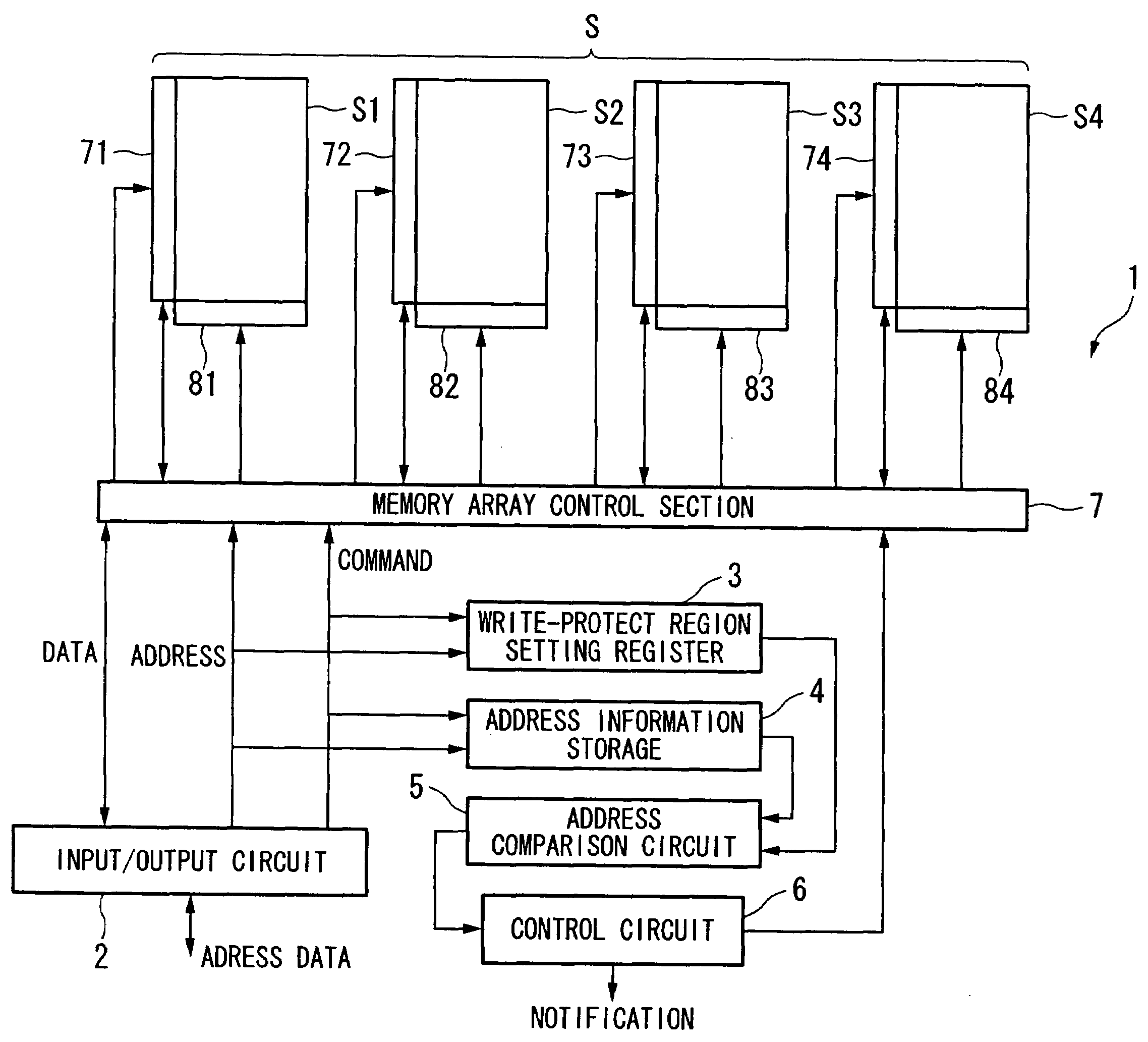
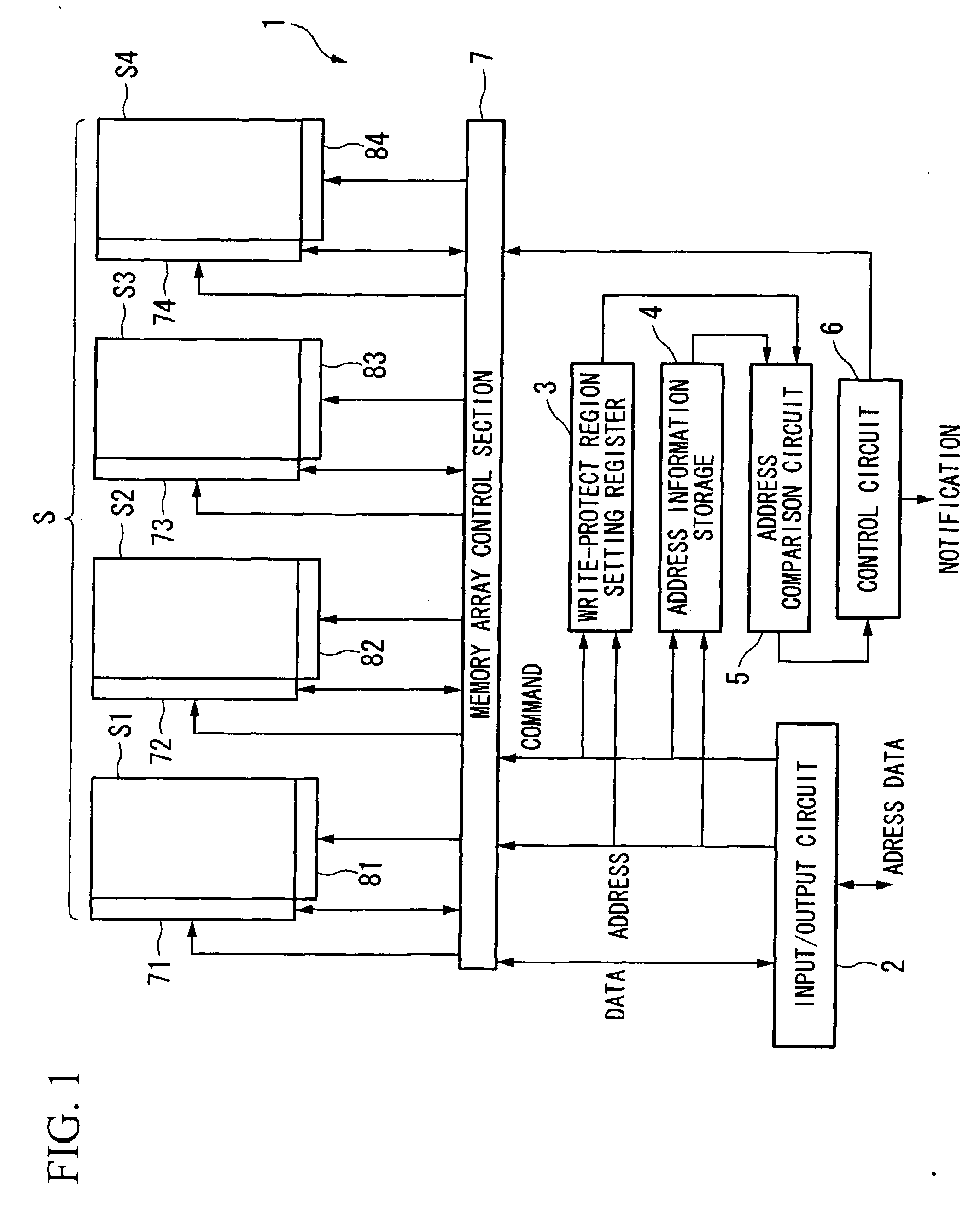
[0052]A nonvolatile RAM 1 according to a preferred embodiment of the present invention will be described with reference to the accompanying drawings. FIG. 1 is a block diagram showing the overall constitution of the nonvolatile RAM 1.

[0053]The nonvolatile RAM 1 of FIG. 1 includes an input / output circuit 2, a write-protect region setting register 3, an address information storage 4, an address comparison circuit 5, a control circuit 6, a memory array control section 7, column decoders 71 to 74, row decoders 81 to 84, and a memory area S.

[0054]The input / output circuit 2 performs input processing on data, commands, addresses, and it also performs output processing on data read from memory cells (or memory elements).

[0055]The memory area S is divided into plural areas, i.e., four memory arrays S1, S2, S3, and S4.

[0056]Th...


PUM


Abstract

A nonvolatile RAM for reading and writing data in a random manner includes a memory area configured by a plurality of memory cells suited to a nonvolatile-mode write operation, in which the stored content thereof is not lost irrespective of a power-off event, and a volatile-mode write operation, in which the stored content thereof is lost in the power-off event. A register designates a first portion of the memory area adapted to the nonvolatile-mode write operation regarding fixed data such as program codes and a second portion of the memory area serving as a work area adapted to the volatile-mode write operation. A control circuit performs the nonvolatile-mode write operation on the first portion of the memory area while performing the volatile-mode write operation on the second portion of the memory area.

Description

BACKGROUND OF THE INVENTION[0001]1. Field of the Invention[0002]The present invention relates to nonvolatile memory such as nonvolatile random-access memory (RAM), whose data are not lost irrespective of power-off events and which can be accessed in a random manner.[0003]This application claims priority on Japanese Patent Application No. 2007-42230, the content of which is incorporated herein by reference.[0004]2. Description of the Related Art[0005]Conventionally, various types of nonvolatile memory such as flash memory (e.g., read-only memory (ROM) reloadable by user on board) have been known. For example, Japanese Unexamined Patent Application Publication No. 2001-14871 teaches a flash memory having security and protection functions.[0006]In general, in the computer system adapted to cellular phones as shown in FIGS. 10 and 11, program codes are stored on hard disks or reloadable ROM such as flash memory in connection with processors, wherein program codes are loaded into and exe...

Claims


Application Information

Patent Timeline
IPC IPC(8): G11C16/04G11C7/00
CPCG11C14/00
Inventor KAJIGAYA, KAZUHIKO
Owner LONGITUDE SEMICON S A R L
Learn More