Organic electroluminescent display device and fabrication method thereof
- Summary
- Abstract
- Description
- Claims
- Application Information
AI Technical Summary
Benefits of technology
Problems solved by technology
Method used
Image
Examples
first embodiment
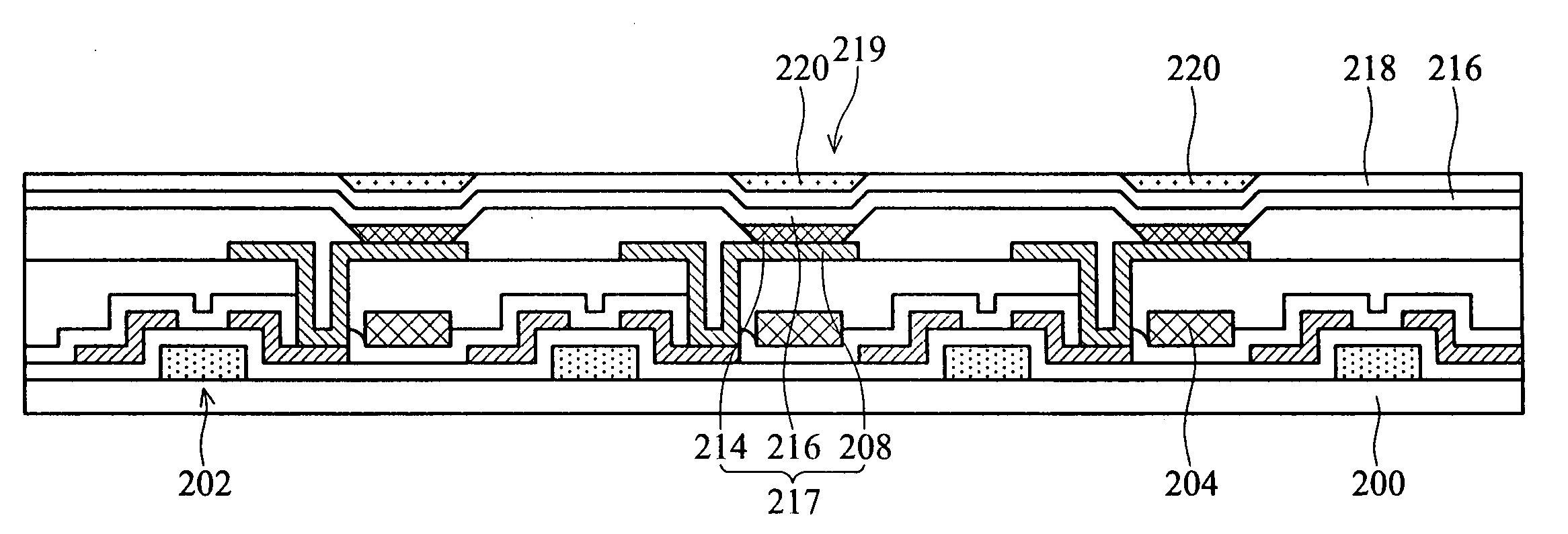
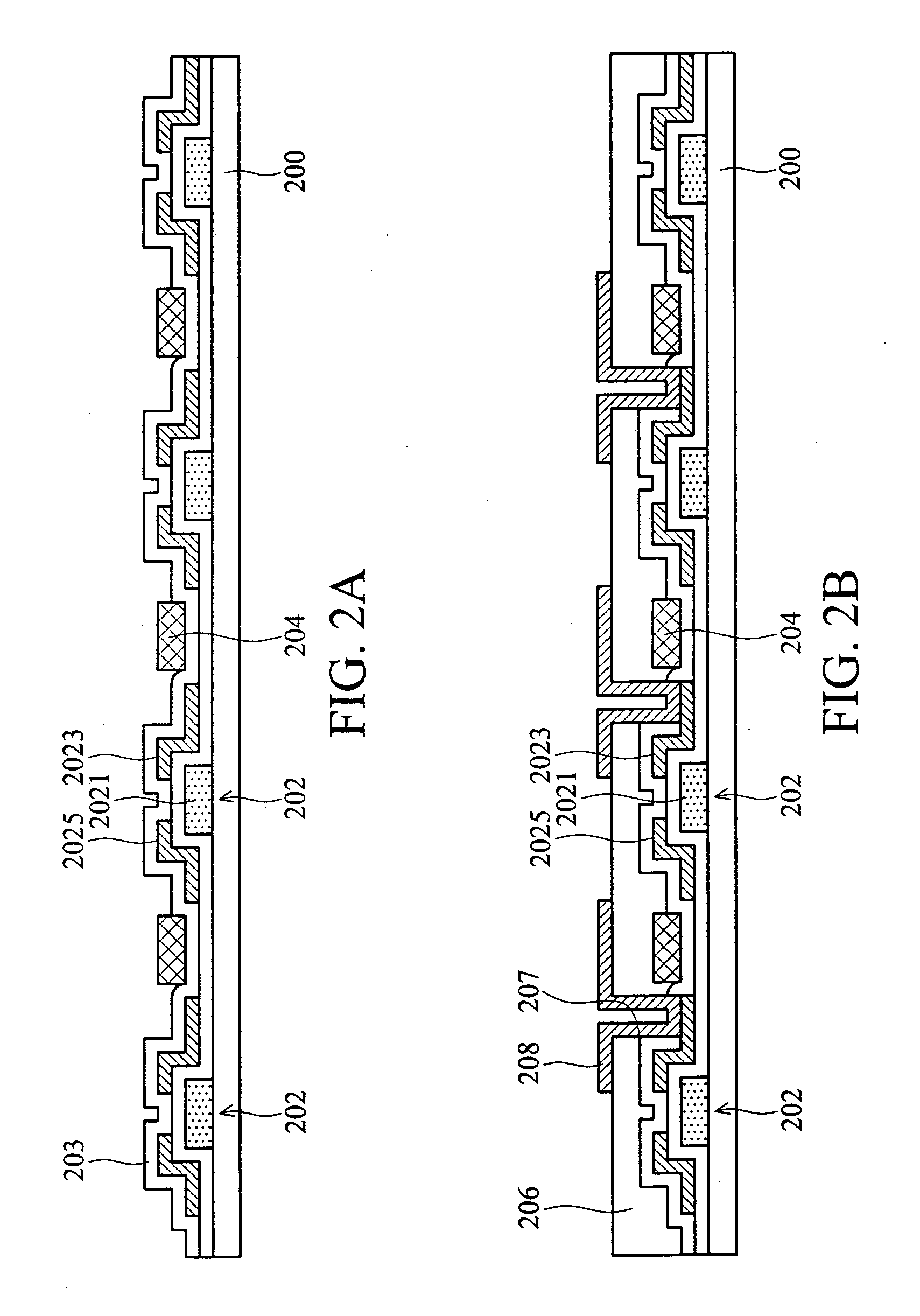
[0019]FIG. 2A through FIG. 2H, show cross-sectional views of forming an organic electroluminescent display device according to the invention. In this embodiment, a color filter and thin film transistor serving as a switch may be disposed on the same substrate in the organic electroluminescent display device. That is, the color filter may be formed on the substrate on which the thin film transistor is formed.
[0020]As shown in FIG. 2A, a color filter 204 is formed on a first substrate 200 having a plurality of thin film transistors (TFTs) 202 formed thereon. The first substrate 200 is transparent material, such as, glass or plastic. The flexible transparent material may also be used in first substrate 200.
[0021]The thin film transistor 202, serving as a switch, includes a gate electrode 2021, a source 2025 and drain 2023, in which the gate electrode 2021 is formed on the first substrate 200 followed by formation of the source 2025 and drain 2023 thereon. The gate electrode, source and...
second embodiment
[0054]The organic electroluminescent display device of the invention effectively prevents oxidation of electrodes by infiltration of moisture into the electroluminescent unit. Because the first protective layer comprising inorganic material, the second protective layer comprising organic material and the third protective layer comprising inorganic material are formed on the electroluminescent unit to prevent moisture infiltration. Additionally, a stress between the first protective layer comprising inorganic material and the third protective layer comprising inorganic material is reduced by forming the second protective layer comprising organic material therebetween. Furthermore, the second protective layer is only formed in the recess over the electroluminescent unit, thus, fabrication cost is reduced. Furthermore, waterproof ability of the organic electroluminescent display device is enhanced without increasing thickness of the organic electroluminescent display device because th...
third embodiment
[0058]A third protective layer 422 is then formed on the second protective layer 420 and in contact with the first protective layer 418 after the second protective layer 420 is formed. Finally, a second substrate 428 is sealed to the first substrate 400 by a sealant 426. A buffer layer 424 is filled between the first substrate 400 and second substrate 428, to complete an organic electroluminescent display device according to the invention, as shown in FIG. 4.
[0059]Note that color filter and shielding layer is not necessarily formed on the second substrate, thus, steps of fabrication and cost of material utilized are reduced. A stress between the first protective layer comprising an inorganic material and third protective layer comprising an inorganic material is reduced because the second protective layer comprises an organic photoresist. Note that the second protective layer in first embodiment may be a material of organic color photoresist function as protective layer and color fi...
PUM
 Abstract
Description
Claims
Application Information


