Semiconductor device

Active Publication Date: 2008-09-11
RENESAS ELECTRONICS CORP
View PDF2 Cites 13 Cited by
  • Summary
  • Abstract
  • Description
  • Claims
  • Application Information

AI Technical Summary

Benefits of technology

[0013]As has been described, the present invention makes it possible to reduce the defect of a ball and a BGA substrate falling apart from each other during or after assembly. A possible mechanism of this defect is as follows:
[0014]An edge of a semiconductor chip is the interface between the semiconductor chip and packaging resin. Distortion from stress generated on the interface, especially stress due to heat, concentrates on the interface. Furthermore, the concentrated stress increases the stress difference among a BGA substrate, a solder ball, and a secondary packaging substrate which are under the interface, until the concentrated stress ultimately separates the solder ball from a landing pad. Placing the interface off an imaginary line extended from the landing pad therefore reduces the above defect exponentially.
[0015]The above placement also mitigates limitation on chip size for semiconductor devices. Specifically, although the solder ball position in the semiconductor device to be mounted to the secondary packaging substrate is fixed with respect to the wiring pattern on the secondary packaging substrate, and this may put an edge of the semiconductor chip at the above-described solder ball position, no problems arise if the semiconductor chip is mounted to the packaging substrate such that the semiconductor chip center is offset from the center of the packaging substrate (will be called eccentric mounting).
[0016]Eccentric mounting, which provides an increased degree of freedom in chip size, also makes it easy to deal with simple chip shrinking or minor changes to th

Problems solved by technology

However, conventional BGA packaging has never given consideration to the positional relation between the edges of a semiconductor chip and balls on a BGA substrate, in

Method used


Image

  • Semiconductor device
  • Semiconductor device
  • Semiconductor device

Examples


first embodiment

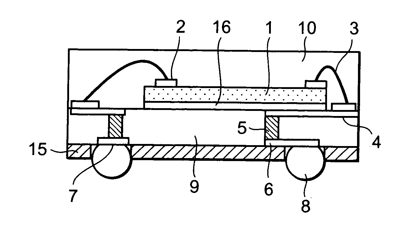
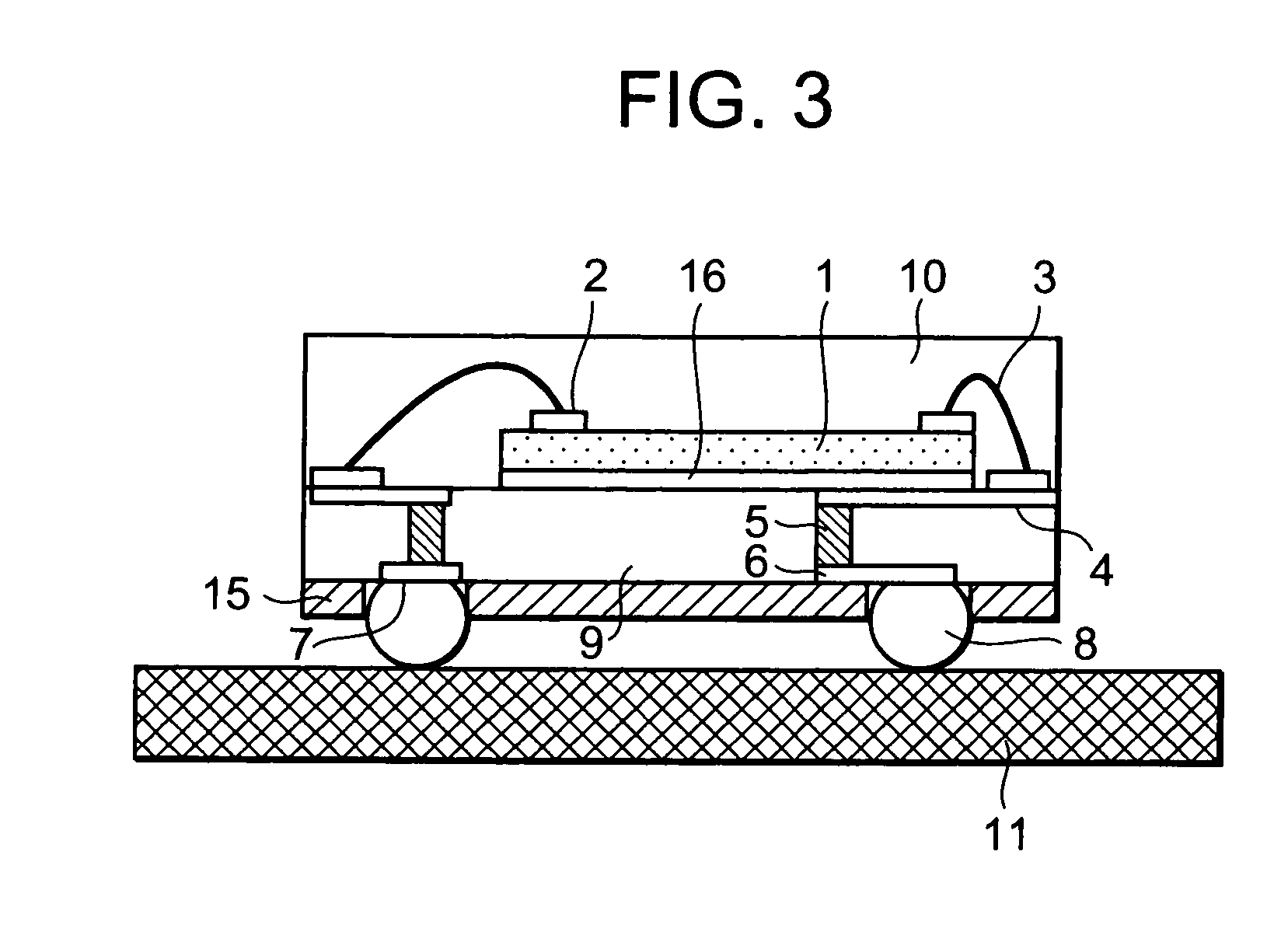
[0037]The above embodiment takes assembly by bonding as an example. A modification example of the present invention is shown in FIG. 5. In the modification example, the semiconductor chip 1 is a flip chip and pads 2 on the flip chip are press-fit to the BGA substrate 9 through metal bumps 12. The semiconductor chip 1 in this case, too, is positioned such that semiconductor chip edges do not align with the solder ball centers as in the above embodiment.

second embodiment

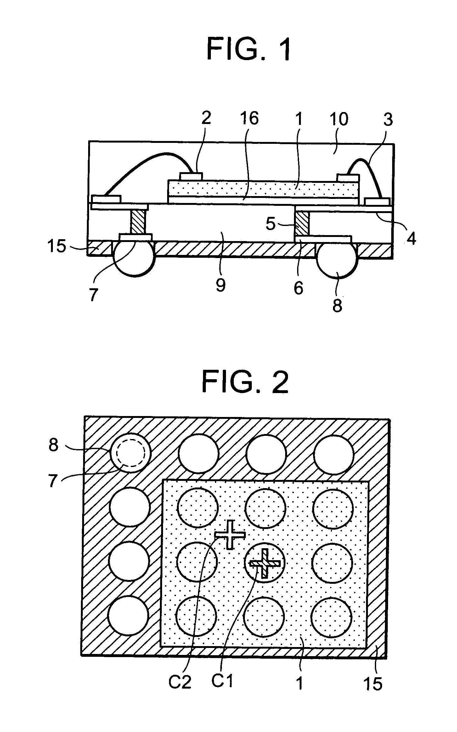
[0038]FIGS. 6 and 7 are diagrams showing a semiconductor device according to the present invention.

[0039]In FIG. 6, a semiconductor chip 13 is layered over the semiconductor chip 1 of the first embodiment of the present invention, thereby making a multi-chip package (MCP) structure. The two layered semiconductor chips are arranged such that their respective edges do not align with the ball positions on the BGA substrate in, the perpendicular direction as in the first embodiment of the present invention. This will be described below with reference to FIG. 7, which is a diagram visualizing a planar perspective view of the chip from above the chip.

[0040]The center of the lower semiconductor chip 1 and the center of the upper semiconductor chip 13 coincide with each other in this embodiment. Depending on the chip size of the upper chip, or the chip aspect ratio, however, the centers of the upper and lower semiconductor chips must not coincide with each other.

[0041]FIG. 8 is a modificati...


PUM


Abstract

When a BGA package device is mounted to another substrate and tested for packaging strength, solder balls (8) frequently come detached in places where the edges of a semiconductor chip (1) align with the centers of the solder balls (8) on a BGA substrate (9) in the perpendicular direction of the substrate. In a semiconductor device of the present invention, the center of a semiconductor chip and the center of a BGA substrate to which the chip is mounted do not coincide with each other, and edges of the semiconductor chip do not align with the ball center positions on the BGA substrate in a direction perpendicular to the chip.

Description

BACKGROUND OF THE INVENTION[0001]1. Field of the Invention[0002]The present invention relates to a semiconductor device and, more particularly, to a semiconductor device with a ball grilled array (BGA) substrate in which a semiconductor chip is packaged.[0003]2. Description of the Related Art[0004]There has lately been an increasing demand for semiconductor devices used in mission-critical communication equipment and high-end computers to be faster and to have higher performance. To meet the demand, semiconductor chips and semiconductor devices in which semiconductor chips are packaged have to be reduced in size. One of miniaturization solutions is BGA packaging.[0005]Techniques that revolve around bonding structures for bonding a BGA package and a circuit substrate are found in, for example, JP 2001-144214 A.[0006]This publication discloses a semiconductor device and its bonding structure which prolong the bonding lifetime by giving metal balls that are on the perimeter a higher te...

Claims


Application Information

Patent Timeline
IPC IPC(8): H01L23/488
CPCH01L23/49816H01L23/49838H01L24/48H01L2924/15311H01L2225/06568H01L2225/0651H01L2224/73265H01L2224/48227H01L2224/48091H01L2224/32225H01L2224/32145H01L2924/00014H01L2924/00H01L2924/00012H01L24/73H01L2924/15183H01L2924/181H01L2224/45099H01L2224/45015H01L2924/207
Inventor NIKAIDO, HIROFUMI
Owner RENESAS ELECTRONICS CORP
Why Eureka
Try Eureka