Apparatus and method for reducing edge effect in an image sensor

Active Publication Date: 2008-09-11
SAMSUNG ELECTRONICS CO LTD
View PDF10 Cites 33 Cited by
  • Summary
  • Abstract
  • Description
  • Claims
  • Application Information

AI Technical Summary

Benefits of technology

[0010]In general, dummy pixels are disclosed that exhibit identical electrical characteristics to any other pixel in the imaging array. This insures that the total current of each dummy pixel used in an array also containing clear pixels and OB pixels is roughly identical to the total current of a clear pixel. While an OB pixel used as a reference for signal processing is read each frame, a dummy pixel must look the same even though it may never be read, regardless whether it is opaque or light-sensitive. Further, the dummy pixels do not perturb the electrical characteristics of nearby pixels so that they can be used to isolate the various sub-arrays that compose an imaging array. Such dummy pixels are also placed at the edges of the imaging array to prevent discontinuities stemming from process-related, physical and electrical factors. Edge effects are thereby eliminated.
[0014]2) partitioning the pixel array into sub-arrays of clear pixels, dummy pixels, and OB pixels that may be isolated from supporting peripheral circuits by N-guard band regions. The latter guard band regions collect stray minority carriers and prevent extraneous minority carriers from offsetting the OB reference signal. Such guard bands are used in areas adjacent to, for example, high speed digital circuits that emit light as a by-product of hot carrier effects.
[0015]In addition to these two steps, dummy OB pixel formation is completed by operating the dummy pixels with the reset transistor biased in soft reset mode to prevent signal integration. This insures low-noise operation and minimizes generation of excess generation-recombination currents that alter diode ideality and / or RoA product.
[0016]Dummy clear pixel formation is completed by omitting step 1 and again operating these pixels with the reset transistor biased in soft reset mode. Dummy clear pixels are the main guard bands protecting the imaging array from deleterious edge effects since the omission of the OB step results in the best possible electrical match to the clear pixels in the imaging array.

Problems solved by technology

In addition to the difficulty in achieving the necessary opacity in OB pixels without perturbing electrical characteristics, there is also a need for forming dummy pixels that generate the same nominal current as OB pixels and clear pixels.

Method used


Image

  • Apparatus and method for reducing edge effect in an image sensor
  • Apparatus and method for reducing edge effect in an image sensor
  • Apparatus and method for reducing edge effect in an image sensor

Examples


Embodiment Construction

[0030]The following description is provided to enable any person skilled in the art to make and use the invention and sets forth the best modes contemplated by the inventor for carrying out the invention. Various modifications, however, will remain readily apparent to those skilled in the art. Any and all such modifications, equivalents and alternatives are intended to fall within the spirit and scope of the present invention.

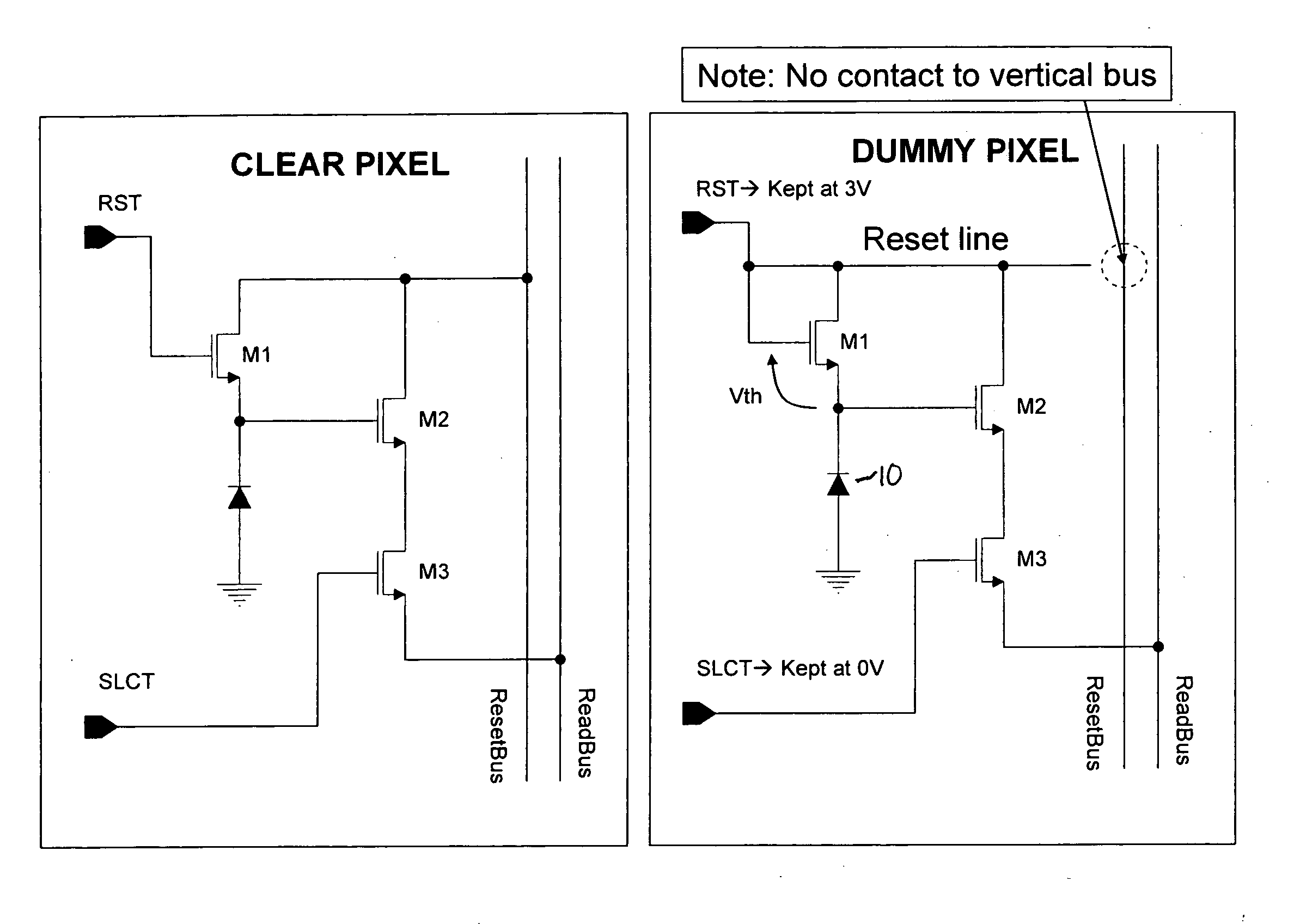
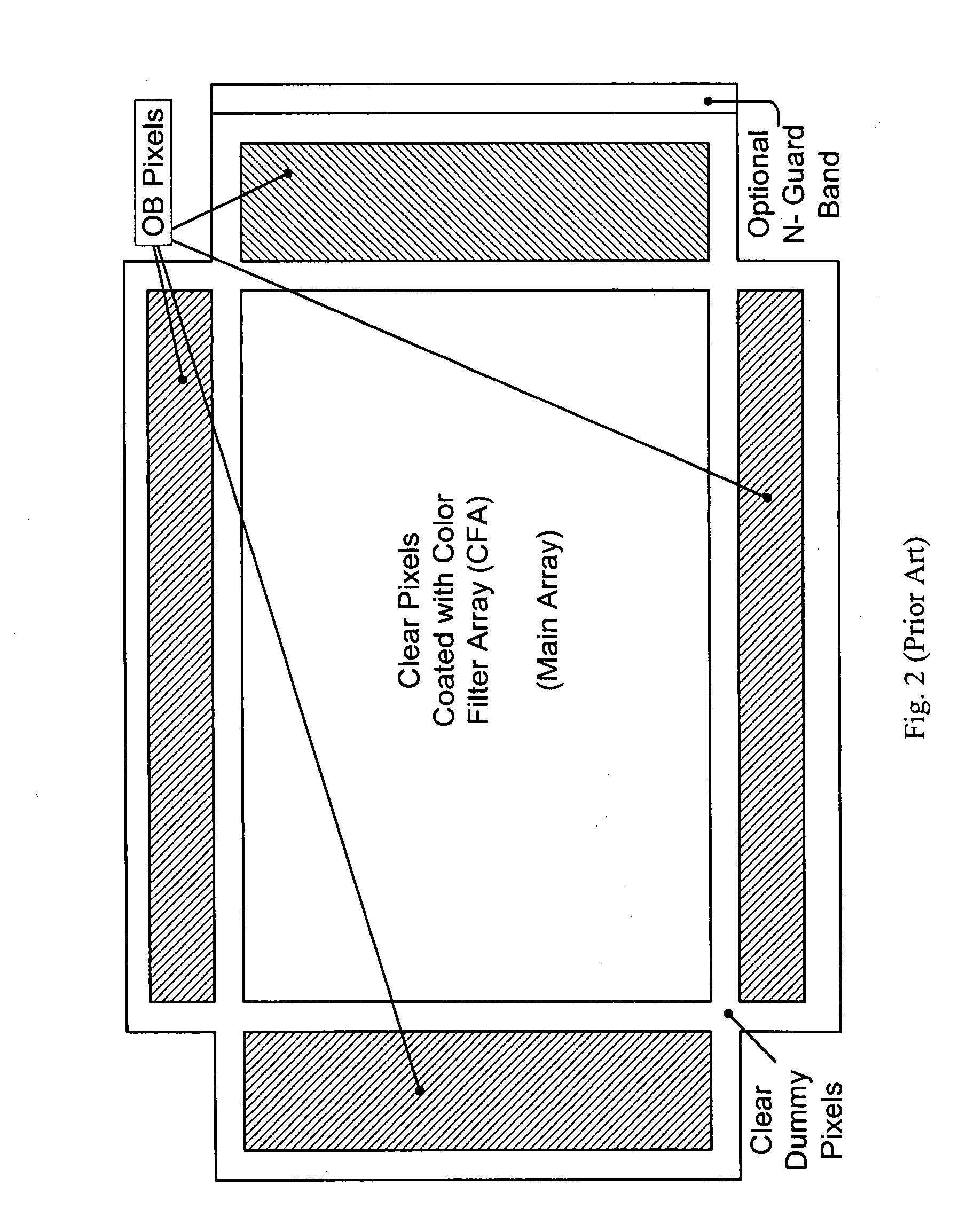
[0031]In general, the present invention provides clear dummy pixels and Optical Black (OB) dummy pixels having virtually identical electrical characteristics as the clear pixels in the imaging sensor. The dummy pixels are not necessarily read out but form isolation regions within the array that do not create regional discontinuities resulting in edge effects. The dummy pixels are free of the impediments of existing techniques that complicate sensor design and production. Specifically, the Shockley currents generated in the dummy pixels of the various embodiment...


PUM


Abstract

A method and apparatus for forming dummy pixels exhibiting electrical characteristics virtually identical to the clear pixels of the imaging array. Arrays of such dummy pixels are used to form regions that isolate the main imaging array and sub-arrays of optical black pixels while preventing edge effects. The dummy pixels are preferably clear but can also be covered with optical black. By setting quiescent operation in soft reset, the dummy pixels exhibit the diode ideality and RoA product that are typical of any of the pixels in the entire array.

Description

BACKGROUND OF THE INVENTION[0001]1. Field of the Invention[0002]The present invention relates generally to image processing for electronic imaging sensors, and more particularly, to an apparatus and method for equalizing the dark current in pixels located on the periphery of an image sensor and thereby eliminating the so-called “edge effect” to optimize image quality.[0003]2. Description of the Related Art[0004]Optical black pixels (“OB pixels”) are the reference pixels within an imaging sensor pixel array that should have virtually identical electrical characteristics as a standard active pixel, yet are insensitive to light. OB pixels are used by various image processing circuits in the sensor or camera to maintain a constant black level independent of gain, illumination, changes in sensor operating conditions, etc. An OB pixel's signal is normally processed using the same signal chain and timing as those that are photo-electrically responsive and form the image of interest. The la...

Claims


Application Information

Patent Timeline
IPC IPC(8): H04N9/64
CPCH01L27/14603H04N5/361H01L27/14643H01L27/14609H04N25/63
Inventor ROSSI, GIUSEPPEKOZLOWSKI, LESTER
Owner SAMSUNG ELECTRONICS CO LTD
Why Eureka
Try Eureka