Non-volatile memory

a non-volatile memory and memory technology, applied in the field of semiconductor devices, can solve the problems of affecting the stability and affecting the reliability generating leakage current, so as to improve the reliability and stability of the memory unit, reduce power consumption, and reduce the operation voltage

Inactive Publication Date: 2008-09-18
POWERCHIP SEMICON CORP
View PDF3 Cites 215 Cited by
  • Summary
  • Abstract
  • Description
  • Claims
  • Application Information

AI Technical Summary

Benefits of technology

[0009]Accordingly, the present invention is directed to provide a non-volatile memory unit which avoids the impact of the short channel effect and improves the reliability and stability of the memory unit, and also, the operation voltage can be lowered and the power consumption is reduced.
[0010]Another objective of the present invention is to provide a fabricating method of non-volatile memory, which simplifies the fabricating process, improves the process window and produces memories with higher efficiency.
[0038]As the present invention applies the fin-shaped active layer, and the floating gate and the control gate which cover the active layer, the impact of short channel effect can be avoided; the reliability and stability of the memory are improved; the operation voltage is lowered; and the power consumption is reduced.
[0039]The fabrication method of non-volatile memory according to the present invention not only simplifies the fabrication process, but also reduces the fabrication cost; further, the fabrication process window is improved and the memory with higher efficiency can be made.

Problems solved by technology

Accordingly, the impact of the short channel effect may be more remarkable, which not only changes the on-voltage Vt resulting in the problem of the switch of the path controlled by the gate voltage Vg, but also causes heat electronic effect and punch through effect that a leakage current may be produced in the path or an electrical breakdown may occur.
These problems are adverse for the stability and reliability of the memory unit.
The increase of the operation voltage may lead to more problems such as heat dissipation or noise signal, etc.
; and the power consumption may also be increased.

Method used


Image

  • Non-volatile memory
  • Non-volatile memory
  • Non-volatile memory

Examples


Embodiment Construction

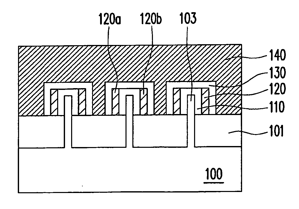
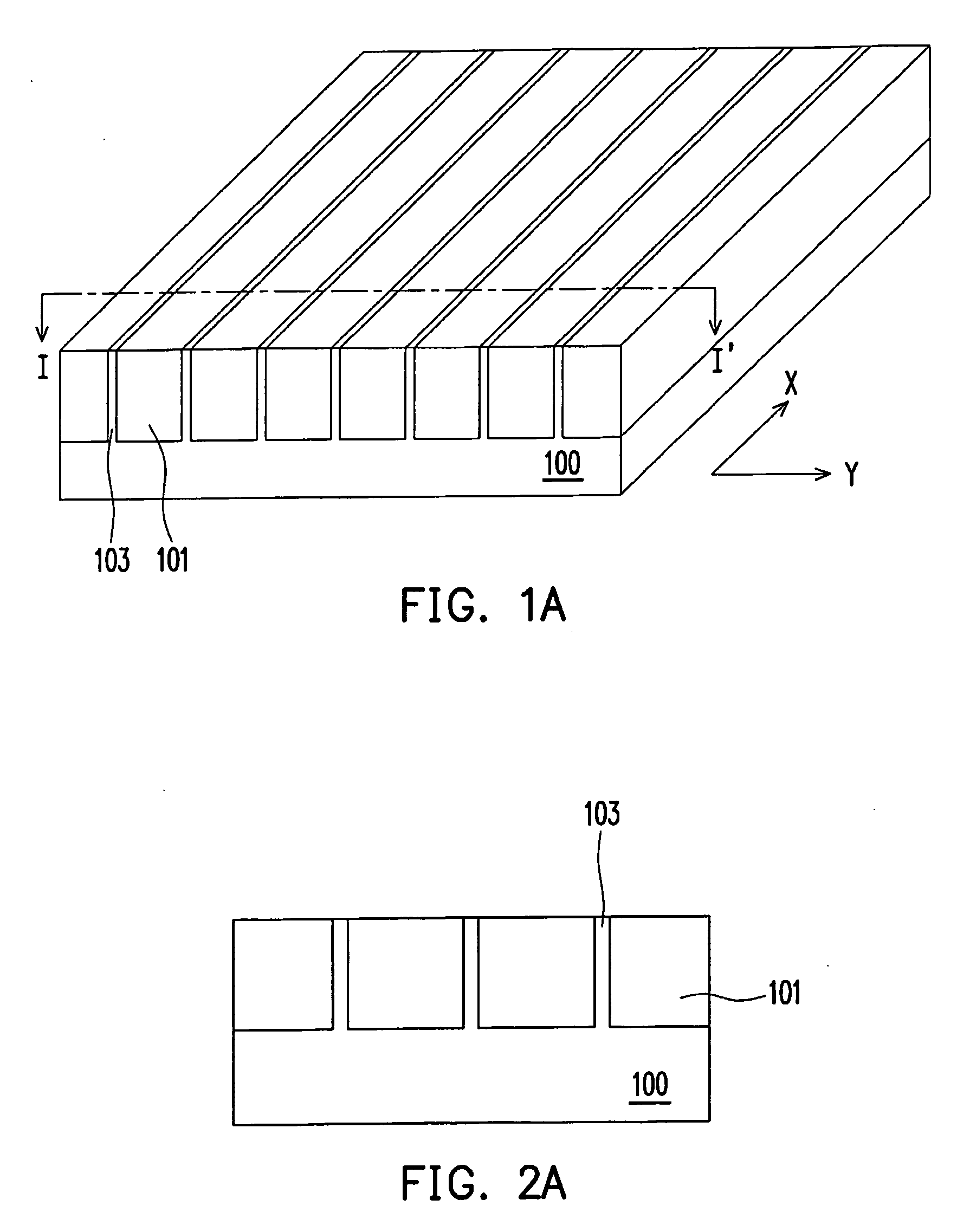
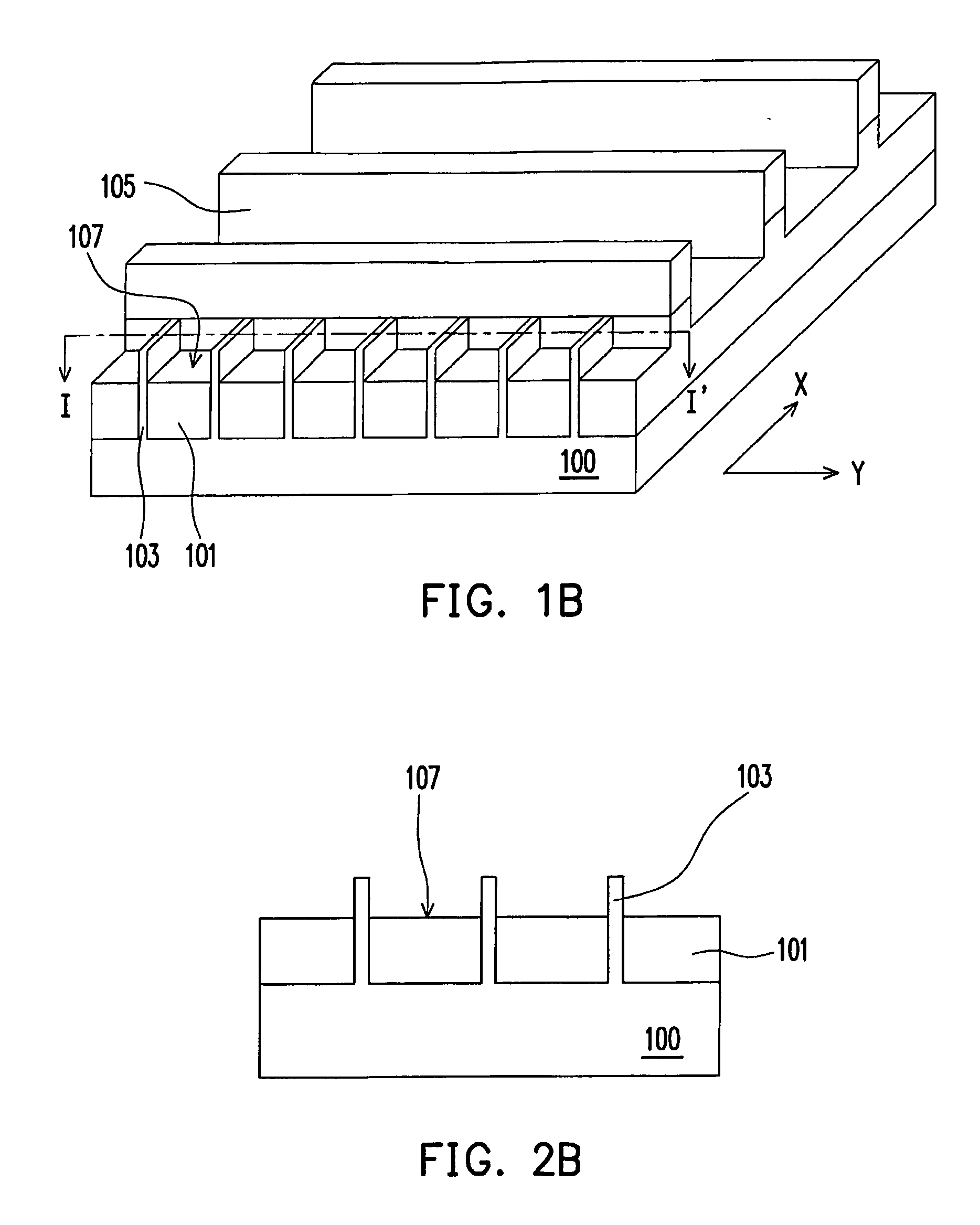
[0048]FIG. 1A to FIG. 1F are tridimensional views of a fabricating process of the non-volatile memory according to one embodiment of the present invention. FIGS. 2A-2F are cross-sectional diagrams of the structures in FIGS. 1A-1F along line I-I′, respectively. FIG. 3E and FIG. 3F are cross-sectional diagrams of the structures in FIG. 1E and FIG. 1F along line II-II′, respectively.

[0049]Referring to FIG. 1A and FIG. 2A, the present invention provides a fabricating method of non-volatile memory, by which an NAND flash memory can be formed. First, a substrate 100 is provided; a plurality of isolation layers 101 is formed on the substrate 100; a plurality of active layers 103 is defined between each isolation layer 101; the active layers 103 and the isolation layers 101 are arranged in parallel to each other and extend in X direction. The substrate 100 is, for example, silicon substrate, or silicon on insulator. The formation method of the isolation layer 101 includes: for example, firs...


PUM


Abstract

A non-volatile memory includes a substrate, a number of isolation layers, a number of active layers, a number of floating gates, a number of control gates and a number of doped regions. The active layers are disposed in the substrate between the isolation layers, and the top surface of the active layer is higher than that of the isolation layer. The active layers and the isolation layers are arranged in parallel to each other and extend in the first direction. The control gates are disposed in the substrate. The control gates are arranged in parallel and extend in the second direction which crosses the first direction. The floating gates are disposed between the active layers and the control gates. The doped regions are disposed in the active layers between the control gates.

Description

CROSS-REFERENCE TO RELATED APPLICATION[0001]This application is a divisional of an application Ser. No. 11 / 306,213, filed on Dec. 20, 2005, now pending, which claims the priority benefit of Taiwan application serial no. 94133689, filed on Sep. 28, 2005. The entirety of the above-mentioned patent applications is hereby incorporated by reference herein and made a part of this specification.BACKGROUND OF THE INVENTION[0002]1. Field of Invention[0003]The present invention relates to a semiconductor device and fabricating method thereof. More particularly, the present invention relates to a non-volatile memory and fabricating method thereof.[0004]2. Description of Related Art[0005]As the flash memory in the non-volatile memory has advantages such as quick and time-saving operation and low cost, it has been one of the main research subjects in the field of art. The typical flash memory mainly includes floating gates and control gates. The control gate is directly disposed on the floating ...

Claims


Application Information

Patent Timeline
Patent Type & Authority Applications(United States)
IPC IPC(8): H01L29/788
CPCH01L27/115H01L29/7851H01L27/11521H10B69/00H10B41/30
Inventor YOUNG, REXWANG, PIN-YAO
Owner POWERCHIP SEMICON CORP
Why Eureka
Try Eureka