Semiconductor device and manufacturing method thereof

a semiconductor device and manufacturing method technology, applied in the direction of semiconductor/solid-state device details, antenna details, antennas, etc., can solve the problems of short communication distance, poor connection, small antenna size, etc., to prevent partial stretching of semiconductor devices, high reliability, and semiconductor elements. high

Inactive Publication Date: 2008-09-18
SEMICON ENERGY LAB CO LTD
View PDF40 Cites 93 Cited by
  • Summary
  • Abstract
  • Description
  • Claims
  • Application Information

AI Technical Summary

Benefits of technology

[0020]By using high-strength fiber as the fibrous body, even when local pressure is applied to a semiconductor device, the pressure is dispersed throughout the fibrous body; accordingly, partial stretching of the semiconductor device can be prevented. That is, destruc...

Problems solved by technology

However, in the case of a semiconductor device with a built-in (on-chip) antenna which is incorporated in a chip, the size of the antenna is small when the size of the chip is small, leading to a problem of a short communication distance.
In the case where a semiconductor device is manufactured by connecting to a chip an antenna provided for a paper medium or a film medium, a poor connection is made when the size of the chip is small.
However, when the area of a chip is enlarged, a semiconductor device which is transferred to a plastic film or the l...

Method used


Image

  • Semiconductor device and manufacturing method thereof
  • Semiconductor device and manufacturing method thereof
  • Semiconductor device and manufacturing method thereof

Examples


embodiment mode 1

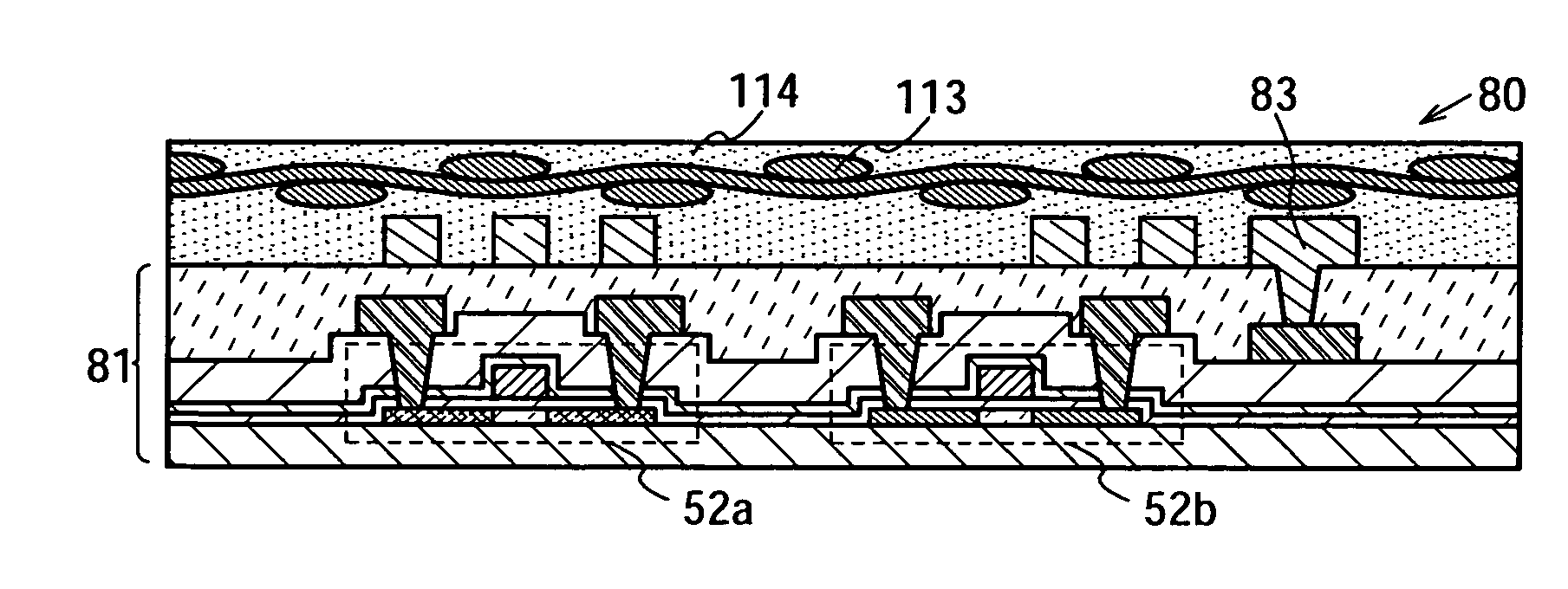
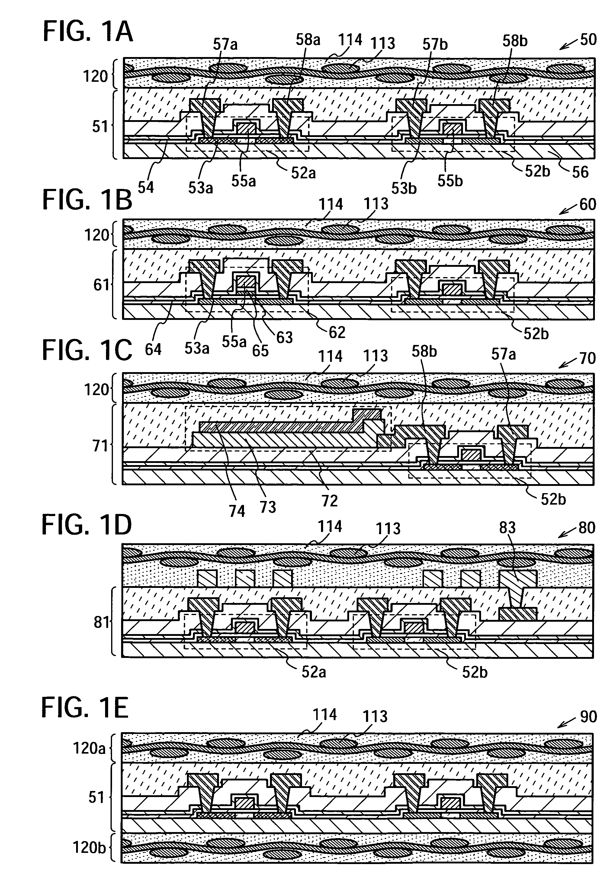
[0039]This embodiment mode describes a highly-reliable semiconductor device which is not easily damaged by local pressure (point pressure, linear pressure, or the like), with reference to FIGS. 1A to 1E, FIGS. 8A and 8B, and FIGS. 9A to 9D.

[0040]One aspect of a semiconductor device of this embodiment mode is that, over an element layer including a semiconductor element formed using a non-single crystal semiconductor layer, a sealing layer including a fibrous body of an organic compound or an inorganic compound and an organic resin with which the fibrous body is impregnated is formed.

[0041]As typical examples of the semiconductor element formed using a non-single crystal semiconductor layer which is included in the element layer, an active element such as a thin film transistor, a diode, or a nonvolatile memory element, and a passive element such as a resistor element or a capacitor element can be given. As the non-single crystal semiconductor layer, a crystalline semiconductor layer...

embodiment mode 2

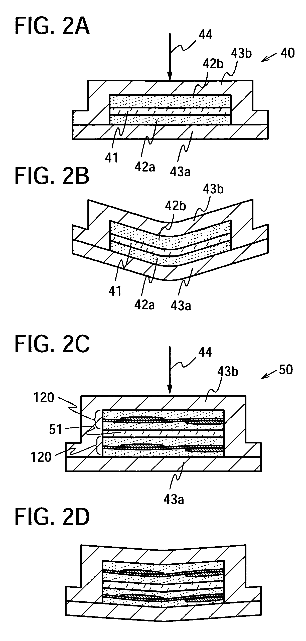
[0086]This embodiment mode describes a method for manufacturing a semiconductor device, which is not easily damaged by external local pressure, with a high yield with reference to FIGS. 3A to 3E.

[0087]As shown in FIG. 3A, a separation layer 101 is formed over a substrate 100 having an insulating surface, and an element layer 102 including a semiconductor element formed using a non-single crystal semiconductor layer and an antenna 112 are formed over the separation layer 101. Then, a structure body 115 in which a fibrous body is impregnated with an organic resin is provided over the element layer 102 and the antenna 112.

[0088]As the substrate 100 having an insulating surface, a substrate which can withstand a temperature at which the element layer 102 and the antenna 112 are formed is preferably used. Typically, a glass substrate, a quartz substrate, a ceramic substrate, a metal substrate in which an insulating layer is formed at least over one surface, an organic resin substrate, or...

embodiment mode 3

[0120]This embodiment mode describes a manufacturing method of a semiconductor device which is not easily destroyed compared with Embodiment Mode 2, with reference to FIGS. 4A to 4D.

[0121]In a similar manner to Embodiment Mode 1, as shown in FIG. 4A, a separation layer 101 is formed over a substrate 100 having an insulating surface, and an element layer 102 including a semiconductor element formed using a non-single crystal semiconductor layer, and an antenna 112 are formed over the separation layer 101. A structure body 115 is provided over the element layer 102 and the antenna 112, and a protective film 131 is provided over the structure body 115.

[0122]The protective film 131 is preferably formed from a high-strength material. As typical examples of a high-strength material, a polyvinyl alcohol resin, a polyester resin, a polyamide resin, a polyethylene resin, an aramid resin, a polyparaphenylene benzobisoxazole resin, a glass resin, and the like can be given.

[0123]Since the prote...


PUM


Abstract

The present invention provides a semiconductor device which is not easily damaged by external local pressure. The present invention further provides a method for manufacturing a highly-reliable semiconductor device, which is not destructed by external local pressure, with a high yield. A structure body, in which high-strength fiber of an organic compound or an inorganic compound is impregnated with an organic resin, is provided over an element layer having a semiconductor element formed using a non-single crystal semiconductor layer, and heating and pressure bonding are performed, whereby a semiconductor device is manufactured, to which the element layer and the structure body in which the high-strength fiber of an organic compound or an inorganic compound is impregnated with the organic resin are firmly fixed together.

Description

BACKGROUND OF THE INVENTION[0001]1. Field of the Invention[0002]The present invention relates to a semiconductor device having a semiconductor element using a non-single crystal semiconductor layer and a manufacturing method of the semiconductor device.[0003]2. Description of the Related Art[0004]Currently, it is important to make various devices, such as wireless chips and sensors, into a thinner shape in miniaturizing products, and the technique and the application range spread rapidly. Such various devices which are made thin are flexible to some extent and thus the devices can be provided for an object having a curved surface.[0005]Therefore, a technique of manufacturing a semiconductor device is proposed, in which an element layer including a thin film transistor which is formed over a glass substrate is separated from the substrate and transferred to another substrate, for example, a plastic film or the like.[0006]The present applicant proposes techniques of separation and tra...

Claims


Application Information

Patent Timeline
IPC IPC(8): H01Q1/40H01L21/02
CPCH01L23/145H01L23/49855H01L2924/07811H01L27/105H01L27/115H01L27/1266H01L27/13H01L29/78603H01L2223/6677H01L2924/09701H01L2924/12044H01Q1/2225H01Q1/2283H01L2224/16225H01L27/1248H01L2924/00H10B69/00H01L27/1214
Inventor SUGIYAMA, EIJIDOZEN, YOSHITAKAOHTANI, HISASHITSURUME, TAKUYA
Owner SEMICON ENERGY LAB CO LTD
Why Eureka
Try Eureka