Light-Emitting Device and Electronic Device

a technology of light-emitting devices and electronic devices, which is applied in the direction of discharge tubes/lamp details, organic semiconductor devices, discharge tubes/lamp details, etc., can solve the problems of difficult to obtain features and damage to the performance of display devices, and achieve excellent characteristics and excellent characteristics

Inactive Publication Date: 2008-09-25
SEMICON ENERGY LAB CO LTD
View PDF40 Cites 85 Cited by
  • Summary
  • Abstract
  • Description
  • Claims
  • Application Information

AI Technical Summary

Benefits of technology

[0066]Since a light-emitting device of the present invention has a suitable structure for a light-emitting element for each color, the light-emitting device can have e

Problems solved by technology

This is a feature which is difficult to be obtained by point light sources typified by an incandescent lamp and an LED or linear light sources typified by a fluorescent lamp.
For example, when a li

Method used


Image

  • Light-Emitting Device and Electronic Device
  • Light-Emitting Device and Electronic Device
  • Light-Emitting Device and Electronic Device

Examples


embodiment mode 1

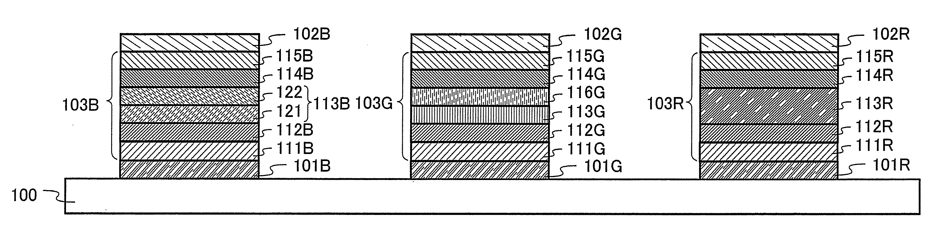
[0101]One mode of a light-emitting device of the present invention will now be described with reference to FIG. 1.

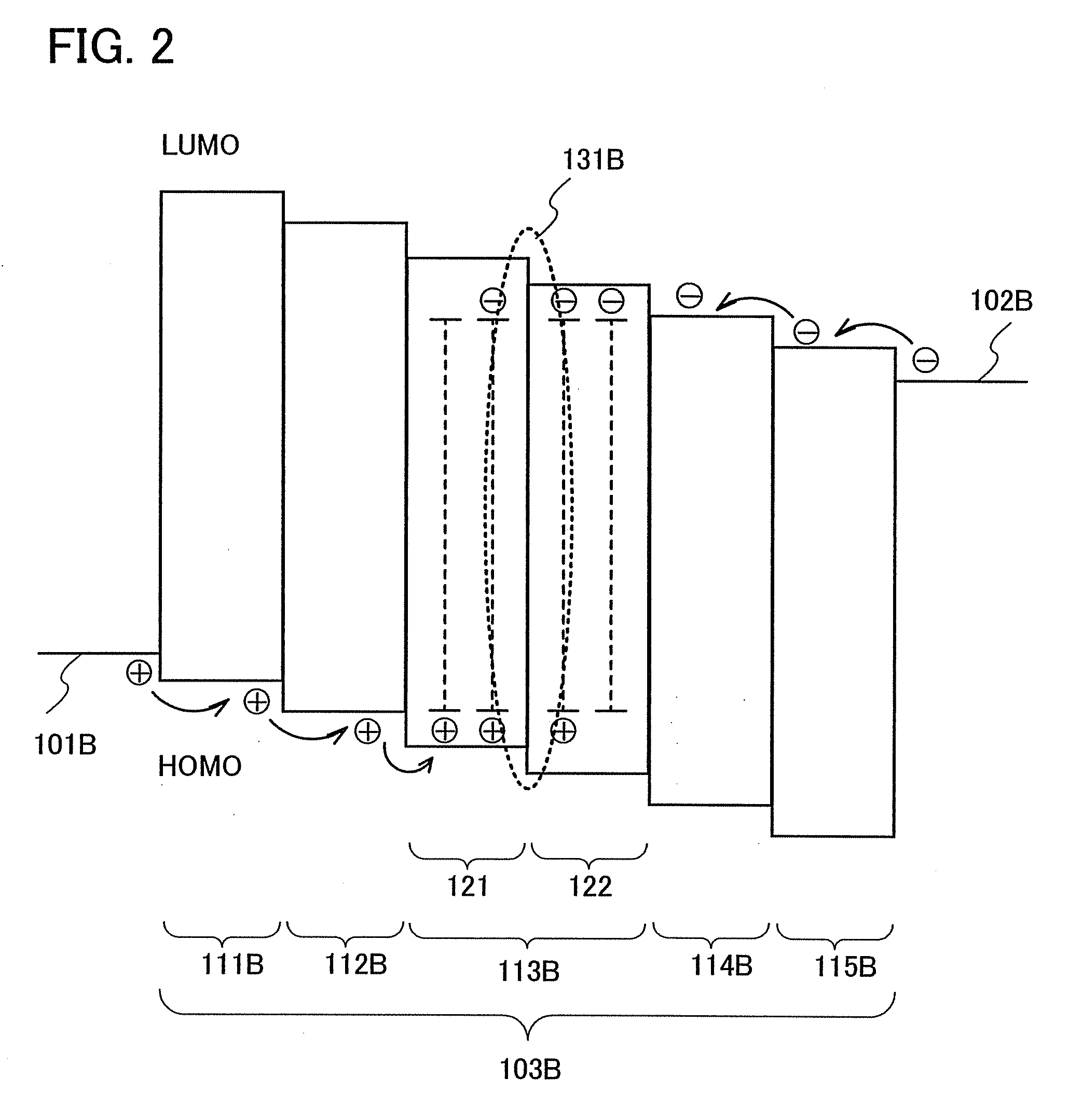
[0102]A light-emitting device of the present invention includes a plurality of light-emitting elements that have an emission color which is different from each other. Each light-emitting element has a plurality of layers between a pair of electrodes. In this specification, the plurality of layers formed between the pair of electrodes are collectively referred to as an EL layer.

[0103]In FIG. 1, a substrate 100 is used as a support of the light-emitting element. The substrate 100 can be glass, plastic or the like, for example. Any material that can serve as a support of the light-emitting element can be used, in addition to the above materials.

[0104]In this embodiment mode, the light-emitting element includes a first electrode, a second electrode, and an EL layer provided between the first electrode and the second electrode. Note that description is made below, on the assu...

embodiment mode 2

[0219]Embodiment Mode 2 will specifically describe a structure of a pyrazine-based organometallic complex which can be used for a light-emitting device of the present invention.

[0220]The pyrazine-based organometallic complex is an organometallic complex which has a ligand having a pyrazine skeleton, and whose a central metal is an element belonging to Group 9 (Co, Rh, Ir) or an element belonging to Group 10 (Ni, Pd, Pt). Further, the organometallic complex should have a property of emitting phosphorescence.

[0221]Many of organometallic complexes belonging to Group 9 or 10 exhibit MLCT (Metal to Ligand Charge Transfer) transition. In particular, the triplet MLCT transition is often observed in phosphorescent compounds. The LUMO level of the organometallic complex exhibiting MLCT transition is determined by the rank of the LUMO level of a ligand. Thus, if a ligand having a high LUMO level is used, the LUMO level of the organometallic complex is also high, and if a ligand having a low L...

embodiment mode 3

[0237]An example of a cross sectional view of a light-emitting device formed according to the present invention will be described with reference to FIG. 9.

[0238]In FIG. 9, a region surrounded by a dashed line represents a transistor 911 which is provided for driving a light-emitting element 912 shown in Embodiment Mode 1. The light-emitting element 912, which is a light-emitting element of the present invention, comprises an EL layer 915 between a first electrode 913 and a second electrode 914. The EL layer 915 has the structure shown in Embodiment Mode 1. A drain of the transistor 911 and the first electrode 913 are electrically connected to each other by a wiring 917 which extends through a first interlayer insulating film 916 (916a, 916b and 916c). The light-emitting element 912 is isolated from other light-emitting elements provided adjacently to the light-emitting element 912 by a partition layer 918. The light-emitting device of the present invention having this structure is p...


PUM


Abstract

The present invention provides light-emitting devices having excellent characteristics and electronic devices having excellent characteristics, having such light-emitting devices. Specifically, the present invention provides a light-emitting device includes a first light-emitting element, a second light-emitting element, and a third light-emitting element which emit light having different color from each other. The first light-emitting element includes a first anode; a first cathode; and a first light-emitting layer and a second light-emitting layer between the first anode and the first cathode, wherein the first light-emitting layer includes a first high light-emitting substance and a first organic compound, and the second light-emitting layer includes the first high light-emitting substance and a second organic compound, wherein the first light-emitting layer is in contact with the first anode side of the second light-emitting layer, and wherein the first organic compound is an organic compound having a hole-transporting property and the second organic compound is an organic compound having an electron-transporting property. The second light-emitting element includes a second anode; a second cathode; and a third light-emitting layer and a layer for controlling carrier transfer between the second anode and the second cathode, wherein the third light-emitting layer includes a second high light-transmitting substance, wherein the layer for controlling carrier transfer includes a third organic compound and a fourth organic compound, and is provided between the third light-emitting layer and the second cathode, wherein the third organic compound is an organic compound having an electron-transporting property and the fourth organic compound is an organic compound having an electron-trapping property; and wherein the third organic compound is included more than the fourth organic compound in the layer for controlling carrier transfer. The third light-emitting element includes a third anode; a third cathode; and a fourth light-emitting layer, wherein the fourth light-emitting layer includes a fifth organic compound, a sixth organic compound, and a third high light-emitting substance, wherein the fifth organic compound is an organic compound having a hole-transporting property, and the sixth organic compound is an organic compound having an electron-transporting property, and wherein the third high light-emitting substance is a substance which emits phosphorescence.

Description

BACKGROUND OF THE INVENTION[0001]1. Field of the Invention[0002]The present invention relates to light-emitting devices and electronic devices having a light-emitting element which utilizes electroluminescence.[0003]2. Description of the Related Art[0004]In recent years, research and development have been actively conducted on light-emitting elements using electroluminescence. In a basic structure of such a light-emitting element, a layer including a substance having a light-emitting property (also referred to as a light-emitting substance) is interposed between a pair of electrodes. By voltage application to this element, light emission can be obtained from the substance having a light-emitting property.[0005]Since such light-emitting elements is of self-light-emitting type, it is considered that the light-emitting elements have advantages over liquid crystal display devices in that visibility of pixels is high, backlight is not required, and so on and is therefore suitable as flat...

Claims


Application Information

Patent Timeline
IPC IPC(8): H01J1/63
CPCC09K11/06H05B33/20C09K2211/1029C09K2211/1044C09K2211/185H01L27/3211H01L51/006H01L51/0061H01L51/0072H01L51/0081H01L51/0085H01L51/5012H01L51/5016H01L2251/552H05B33/14H05B33/18C09K2211/1011H10K59/35H10K85/636H10K85/633H10K85/6572H10K85/324H10K85/342H10K50/11H10K2101/10H10K2101/30H10K50/14
Inventor NOMURA, RYOJISEO, SATOSHIOHSAWA, NOBUHARUSUZUKI, TSUNENORIKAWAKAMI, SACHIKOOSAKA, HARUEINOUE, HIDEKO
Owner SEMICON ENERGY LAB CO LTD
Why Eureka
Try Eureka