Display Device

a display device and display technology, applied in the field of display devices, can solve the problems of charge trapping, big shift of threshold voltage due to charge trapping, etc., and achieve the effects of improving reliability of display devices, suppressing threshold voltage shifts, and improving display devices

Inactive Publication Date: 2008-09-25
SEMICON ENERGY LAB CO LTD
View PDF20 Cites 50 Cited by
  • Summary
  • Abstract
  • Description
  • Claims
  • Application Information

AI Technical Summary

Benefits of technology

[0014]In view of the foregoing problems, the invention is to provide a display device in which reliability of a driver circuit can be improved by suppressing shift of the threshold voltage of a TFT.
[0018]In the invention, voltage applied to a gate of a transistor in a driver circuit is set to a minimum value, so that shift of the threshold voltage of the transistor can be suppressed. Accordingly, reliability of the driver circuit and thus reliability of a display device can be improved. In particular, in a thin film transistor using a thin amorphous semiconductor film, silicon nitride or silicon nitride oxide which has a higher dielectric constant than that of silicon oxide is often used for a gate insulating film in order to secure on current. When silicon nitride or silicon nitride oxide with a high dielectric constant is used, charge tends to be trapped, which leads to shift of the threshold voltage. With a structure of the invention, shift of the threshold voltage can be suppressed, and reliability of the display device can be improved.

Problems solved by technology

Unfortunately, in a thin film transistor including a gate insulating film containing nitrogen, the threshold voltage tends to be largely shifted as an absolute value of voltage applied to a gate is increased and a period of time in an on state (driving time) is increased.
This is because charge is trapped in the gate insulating film when voltage is applied to the gate.
In particular, in a thin film transistor using an amorphous semiconductor, an insulating film containing nitrogen is often used as a gate insulating film, shift of the threshold voltage due to trapping of charge is a big problem.

Method used


Image

  • Display Device
  • Display Device
  • Display Device

Examples


embodiment mode 1

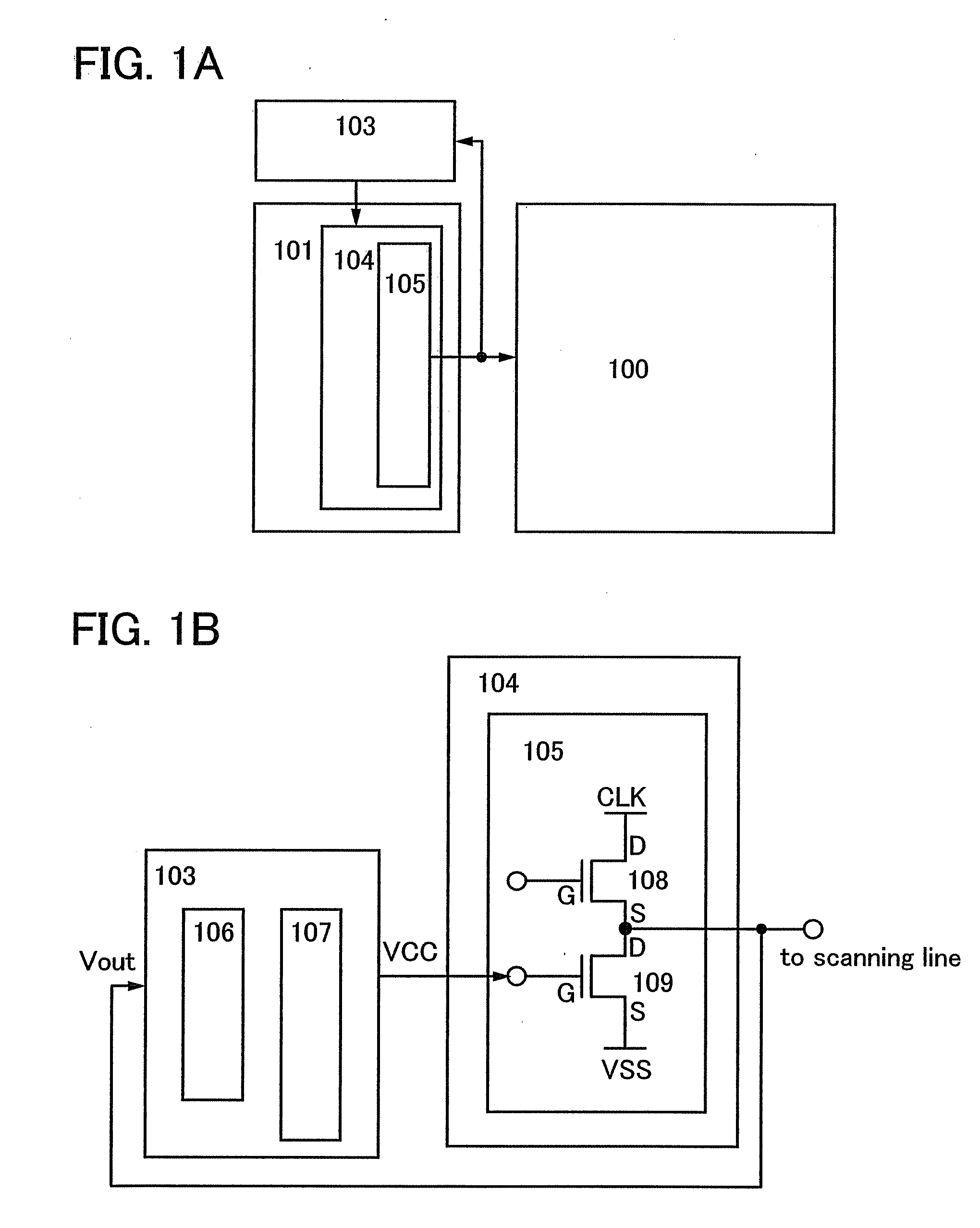
[0037]A structure of a display device of the invention is described with reference to FIGS. 1A and 1B. FIG. 1A is a block diagram of a display device of the invention. The display device of the invention includes a pixel portion 100, a scan line driver circuit 101, and a voltage generation circuit 103. Further, the display device of the invention may include a signal line driver circuit. A plurality of pixels are provided in the pixel portion 100. The pixels in each line are selected by the scan line driver circuit 101. The signal line driver circuit controls input of a video signal to the pixel in the line selected by the scan line driver circuit 101.

[0038]The scan line driver circuit 101 includes a shift register 104. The shift register 104 includes an output circuit 105. The shift register 104 selects a line by using a clock signal CLK and a start pulse signal SP input thereto. Specifically, by controlling switching of the output circuit 105 in accordance with the start pulse sig...

embodiment mode 2

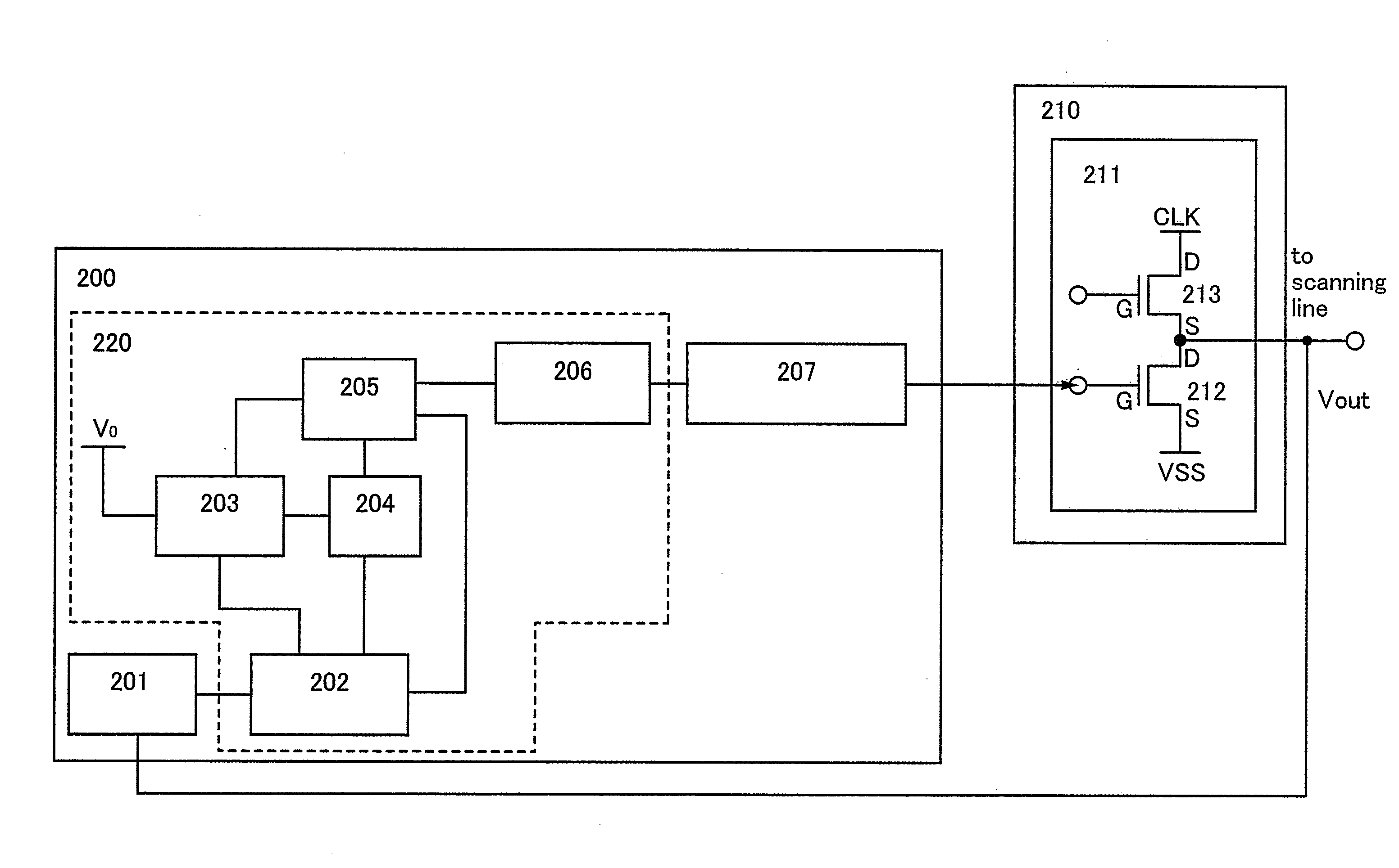
[0056]In this embodiment mode, a specific structure of a voltage generation circuit used in the display device of the invention is described. A voltage generation circuit 200 shown in FIG. 2 includes a decision circuit 201, a voltage setting circuit 220, and an impedance converter 207. The voltage setting circuit 220 includes a controller 202, an adder 203, a counter 204, a switching circuit 205, and a digital-analog (DA) converter circuit 206.

[0057]Note that in FIG. 2, the impedance converter 207 is provided on the output side of the voltage generation circuit 200. Although the impedance converter 207 is not necessarily provided, potential drop due to impedance of a shift register in the next stage can be suppressed with the aforementioned structure. For the impedance converter 207, a voltage follower can be used, for example.

[0058]Next, an operation of the voltage generation circuit 200 shown in FIG. 2 is described. In the voltage setting circuit 220, a value of the voltage VCC ap...

embodiment mode 3

[0067]In this embodiment mode, another structure of a voltage generation circuit used in the display device of the invention, which is different from that in Embodiment Mode 2, is described. A voltage generation circuit 300 shown in FIG. 3 includes a decision circuit 301, a voltage setting circuit 320, and an impedance converter 307. The voltage setting circuit 320 includes a controller 302, an adder 303, a counter 304, and a digital-analog (DA) converter circuit 306.

[0068]Note that in FIG. 3, the impedance converter 307 is provided on the output side of the voltage generation circuit 300. Although the impedance converter 307 is not necessarily provided, potential drop due to impedance of a shift register in the next stage can be suppressed with the aforementioned structure. For the impedance converter 307, a voltage follower can be used, for example.

[0069]Next, an operation of the voltage generation circuit 300 shown in FIG. 3 is described. In the voltage setting circuit 320, a val...


PUM


Abstract

To provide a display device in which reliability of a driver circuit can be improved by suppressing shift of the threshold voltage of a TFT. The minimum power supply voltage that is optimal for driving a transistor used in the driver circuit is found by actually changing voltage applied to a gate of the transistor. Specifically, voltage that is output from an output circuit included in the driver circuit when a value of power supply voltage applied to a shift register is changed is monitored. Then, a value of the power supply voltage is found such that a value of the voltage output from the output circuit satisfies a value enough to operate a pixel portion, and the driver circuit is operated using the power supply voltage.

Description

BACKGROUND OF THE INVENTION[0001]1. Field of the Invention[0002]The present invention relates to a display device using a thin film transistor.[0003]2. Description of the Related Art[0004]In a display device formed using an inexpensive glass substrate, a proportion of a region in the periphery of a pixel portion (a frame region), which is used for mounting, to a substrate is increased as resolution is increased; thus, reduction in size of the display device tends to be prevented. Therefore, it has been considered that a method in which a driver circuit formed using a single crystalline semiconductor substrate is mounted on a glass substrate has limitations, and a technique for forming a driver circuit and a pixel portion over the same glass substrate, that is, so-called system-on-panel has been emphasized. By realization of system-on-panel, the number of pins for connecting a driver circuit and a pixel portion can be reduced, and problems such as reduction in yield due to defective ...

Claims


Application Information

Patent Timeline
Patent Type & Authority Applications(United States)
IPC IPC(8): G06F3/038G09G3/20G09G3/30G09G3/36G11C19/00H01L29/786H01L51/50
CPCG09G3/3266G09G3/3291G09G2300/0408G09G2300/0417H01L51/5237G09G2310/08G09G2330/028H01L27/3276G09G2300/0426H10K59/131H10K50/841G09G3/20G09G3/36G09G3/296G09G3/30
Inventor MIYAKE, HIROYUKIUMEZAKI, ATSUSHI
Owner SEMICON ENERGY LAB CO LTD
Why Eureka
Try Eureka