Optical recording medium and its manufacturing method
- Summary
- Abstract
- Description
- Claims
- Application Information
AI Technical Summary
Benefits of technology
Problems solved by technology
Method used
Image
Examples
first embodiment
(1) First Embodiment
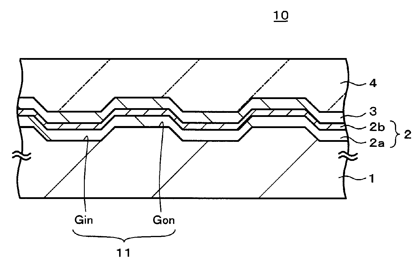
[0023]Construction of optical recording medium FIG. 1 is a schematic cross sectional view showing a constructional example of an optical recording medium according to the first embodiment of the invention. This optical recording medium 10 is what is called a WORM (write once) type optical recording medium and has a construction in which an inorganic recording film 2, a dielectric film 3, and a light transmitting layer 4 are sequentially laminated onto a substrate 1.
[0024]In the optical recording medium 10 according to the first embodiment, an information signal is recorded or reproduced by irradiating a laser beam from the light transmitting layer 4 side onto the inorganic recording film 2. For example, the laser beam having a wavelength within a range from 400 nm or more to 410 nm or less is converged by an objective lens having a numerical aperture within a range from 0.84 or more to 0.86 or less and is irradiated from the light transmitting layer 4 side onto t...
second embodiment
(2) Second Embodiment
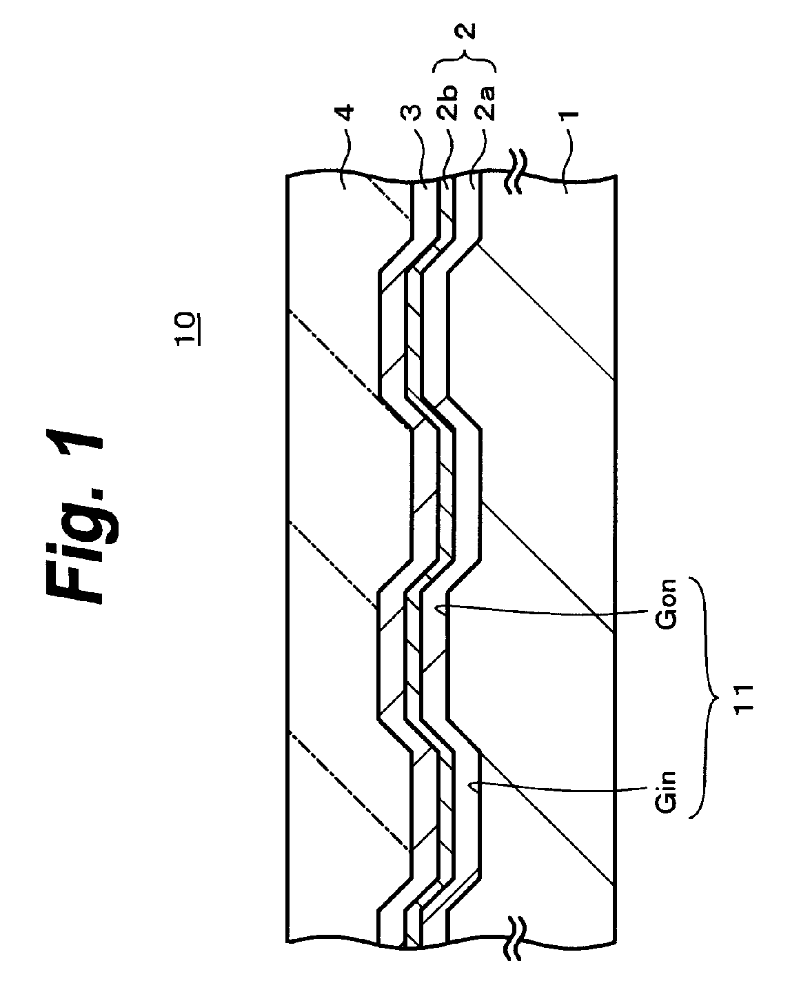
[0072]FIG. 2 is a schematic cross sectional view showing a constructional example of an optical recording medium according to the second embodiment of the invention. According to the second embodiment, the dielectric film 3 in the foregoing first embodiment is constructed by a first dielectric film 3a and a second dielectric film 3b. Portions similar to those in the foregoing first embodiment are designated by the same reference numerals and their explanation is omitted here.
[0073]The first dielectric film 3a is provided on the inorganic recording film 2 side. The second dielectric film 3b is provided on the light transmitting layer 4 side. The first dielectric film 3a and the second dielectric film 3b are made of dielectric substances of, for example, different materials and / or compositions.
[0074]As a material of the first dielectric film 3a, it is preferable to use ZnS—SiO2 from a viewpoint of a film forming speed or the like. A thickness of first dielectric f...
third embodiment
(3) Third Embodiment
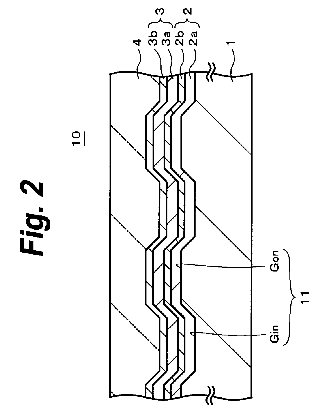
[0092]FIG. 3 is a schematic cross sectional view showing a constructional example of an optical recording medium according to the third embodiment of the invention. The third embodiment has a transparent conductive film 5 between the inorganic recording film 2 and the dielectric film 3. Portions similar to those in the foregoing first embodiment are designated by the same reference numerals and their explanation is omitted here. It is preferable that the transparent conductive film 5 contains at least one kind of SnO2 and In2O3 as a main component. A thickness of transparent conductive film 5 is preferably equal to 1 to 5 nm. If it is equal to 1 nm or more, a power margin can be widened. If it is equal to 5 nm or less, the excellent recording sensitivity can be obtained.
[0093]Subsequently, an example of a manufacturing method of the optical recording medium according to the third embodiment of the invention will be described. Such a manufacturing method of the op...
PUM
| Property | Measurement | Unit |
|---|---|---|
| Thickness | aaaaa | aaaaa |
| Electrical conductor | aaaaa | aaaaa |
| Transparency | aaaaa | aaaaa |
Abstract
Description
Claims
Application Information


