

Carbon nanotube switches for memory, RF communications and sensing applications, and methods of making the same
a technology of carbon nanotubes and switches, applied in nanoelectromechanical switches, relays, instruments, etc., can solve the problems of conventional mems switches having a cyclability problem, multi-throw switching capability at the cost of increasing the on-chip real-estate,
- Summary
- Abstract
- Description
- Claims
- Application Information
AI Technical Summary
Benefits of technology
Problems solved by technology
Method used
Image

Examples
Embodiment Construction
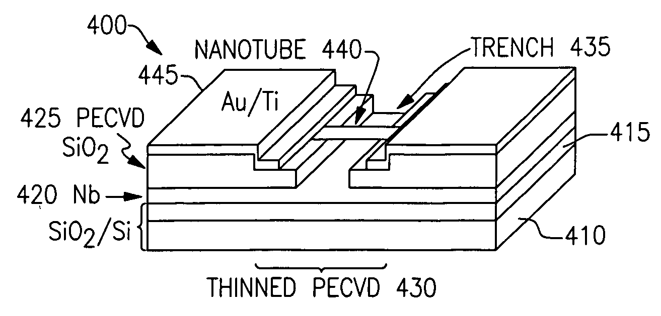
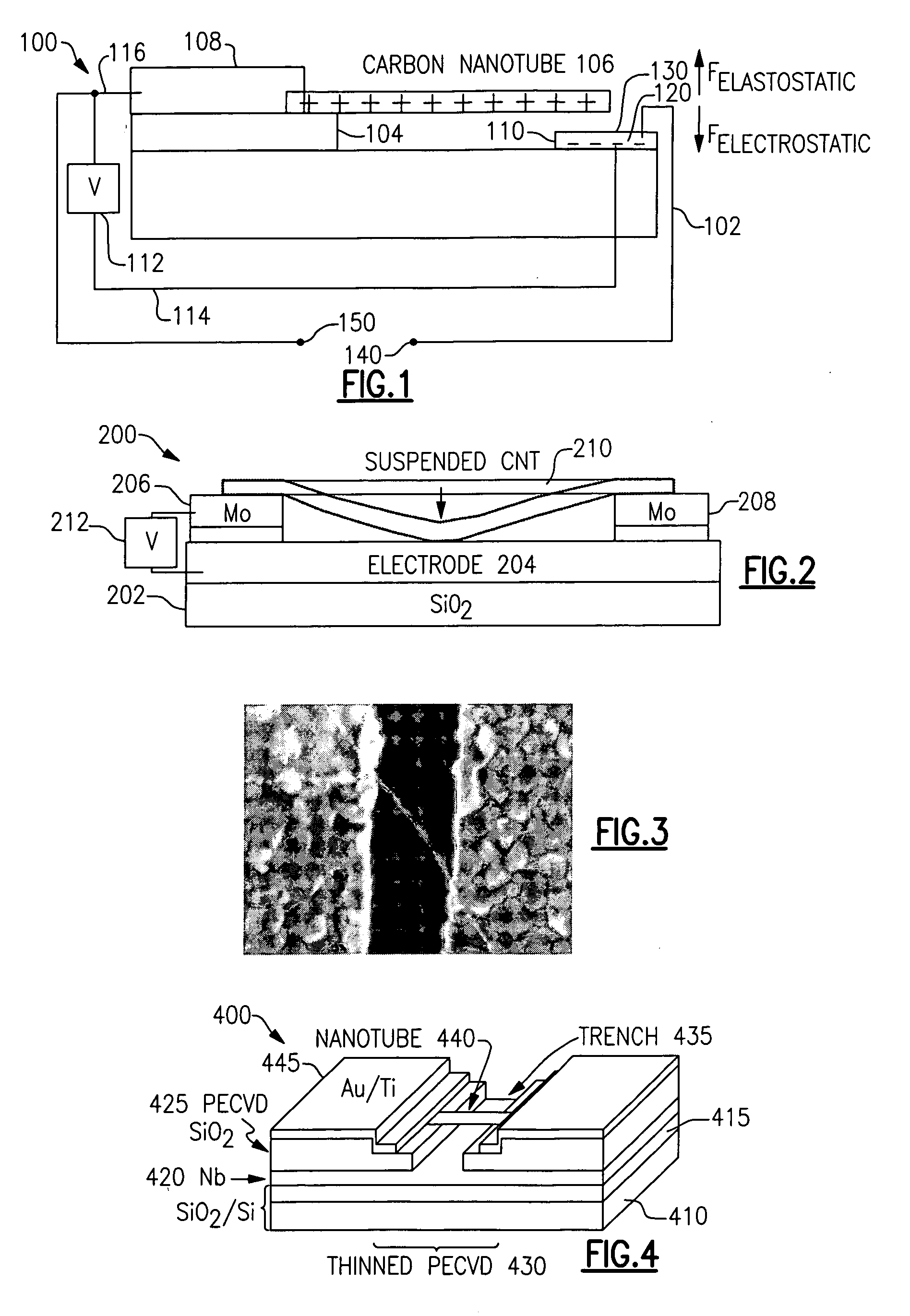
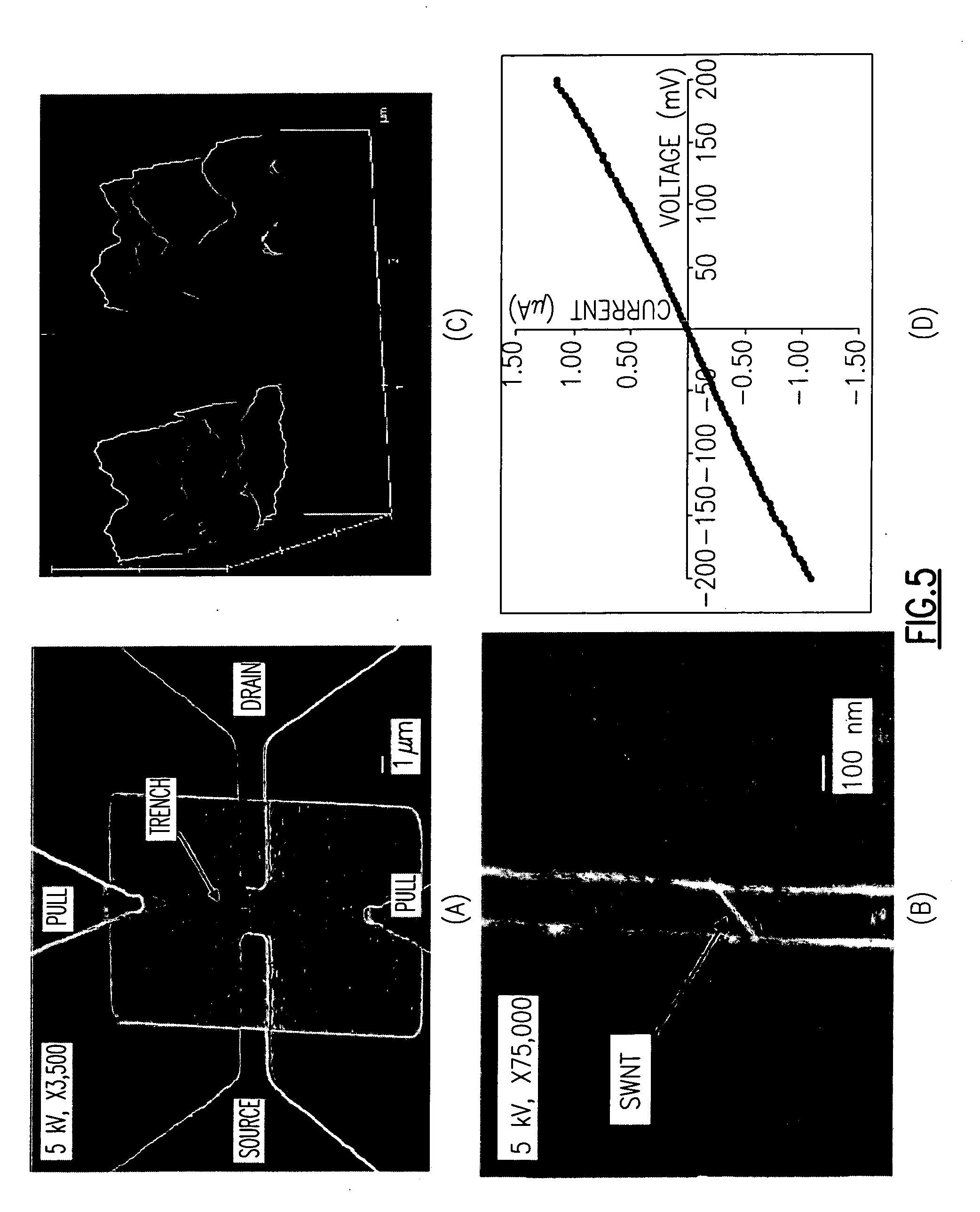
[0061]CNT switches that embody principles of the present invention provide many advantages as compared to conventional CNT switches or conventional NEMS switches. One set of advantages relates to the features of the CNT switches that permit them to be manufactured using materials compatible with high temperature CVD synthesis of CNTs (e.g. refractory metals such as Nb used as an actuating electrode, the use of PECVD SiO2, and as necessary or desirable, the use of other refractory materials such as W, Mo, NbC, and TiN as materials of construction). Since the materials are compatible with high temperature synthesis, the CNT switch can operate as a switch, a memory, and / or a logic element in extreme environments (for example, high temperature environments, harsh chemical environments (due to chemical stability of CNT), and / or high radiation environments) and can be operated at high speed for long periods of time without concern for the potential of generating high temperatures as a con...
PUM
| Property | Measurement | Unit |
|---|---|---|
| temperature | aaaaa | aaaaa |
| temperature | aaaaa | aaaaa |
| temperature | aaaaa | aaaaa |
Abstract
Description
Claims
Application Information