Conversion device, conversion method, program, and recording medium

a conversion device and conversion method technology, applied in the direction of error detection/correction, instruments, detecting faulty computer hardware, etc., can solve the problems of affecting the quality, reliability and manufacturing costs, the output the input wire (pseudo external input wire) cannot be directly accessed from outside, and the controllability of the pseudo external input wire, etc., to achieve the effect of controlling the power consumption of scan capture, deteriorati

Inactive Publication Date: 2008-09-25
JAPAN SCI & TECH CORP +2
View PDF5 Cites 8 Cited by
  • Summary
  • Abstract
  • Description
  • Claims
  • Application Information

AI Technical Summary

Benefits of technology

[0053]According to the present invention, the logic value difference generated before and after the scan capture in the outputs of the scan cells included in the full scan sequential circuit in the logic circuit can be effectively reduced. Accordingly, the scan capture power consumption can be controlled, and any false test can be thereby avoided. Therefore, the deterioration of a percentage of fair products, an example of which is to evaluate a semiconductor logic circuit normally operating at normal times as a defective product in a test and discard it, can be prevented.
[0054]In the conversion device and the conversion method according to the present invention, it is unnecessary to change a test design flow of the logic circuit or increase a circuit area by adding har

Problems solved by technology

A ratio by which the non-defective products can be obtained is called the yielding percentage, and the yielding percentage largely affects the quality, reliability and manufacturing costs of the semiconductor logic circuit.
However, in general, the output wire (pseudo external input wire) and the input wire (pseudo external output wire) of the flip-flop of the sequential circuit cannot be directly accessed from outside.
Therefore, there are problems in the controllability of the pseudo external input wire and the observability of the pseudo external output wire when the combinational circuit unit is tested.
The scan test method described above, which is a very effective means, still includes the problem that more power is consumed in the test than in a normal operation.
In the case where a CMOS circuit constitutes a semiconductor logic circuit, the power consumption includes static power consumption due to leak current and dynamic power consumption due to the switching activity of logic gates and flip-flops.
Further, the latter power consumption, which is the dynamic power consumption, includes shift power consumption in a shift operation and capture power consumption in a capture operatio

Method used


Image

  • Conversion device, conversion method, program, and recording medium
  • Conversion device, conversion method, program, and recording medium
  • Conversion device, conversion method, program, and recording medium

Examples


Embodiment Construction

[0077]Hereinafter, a preferred embodiment of the present invention is shown below.

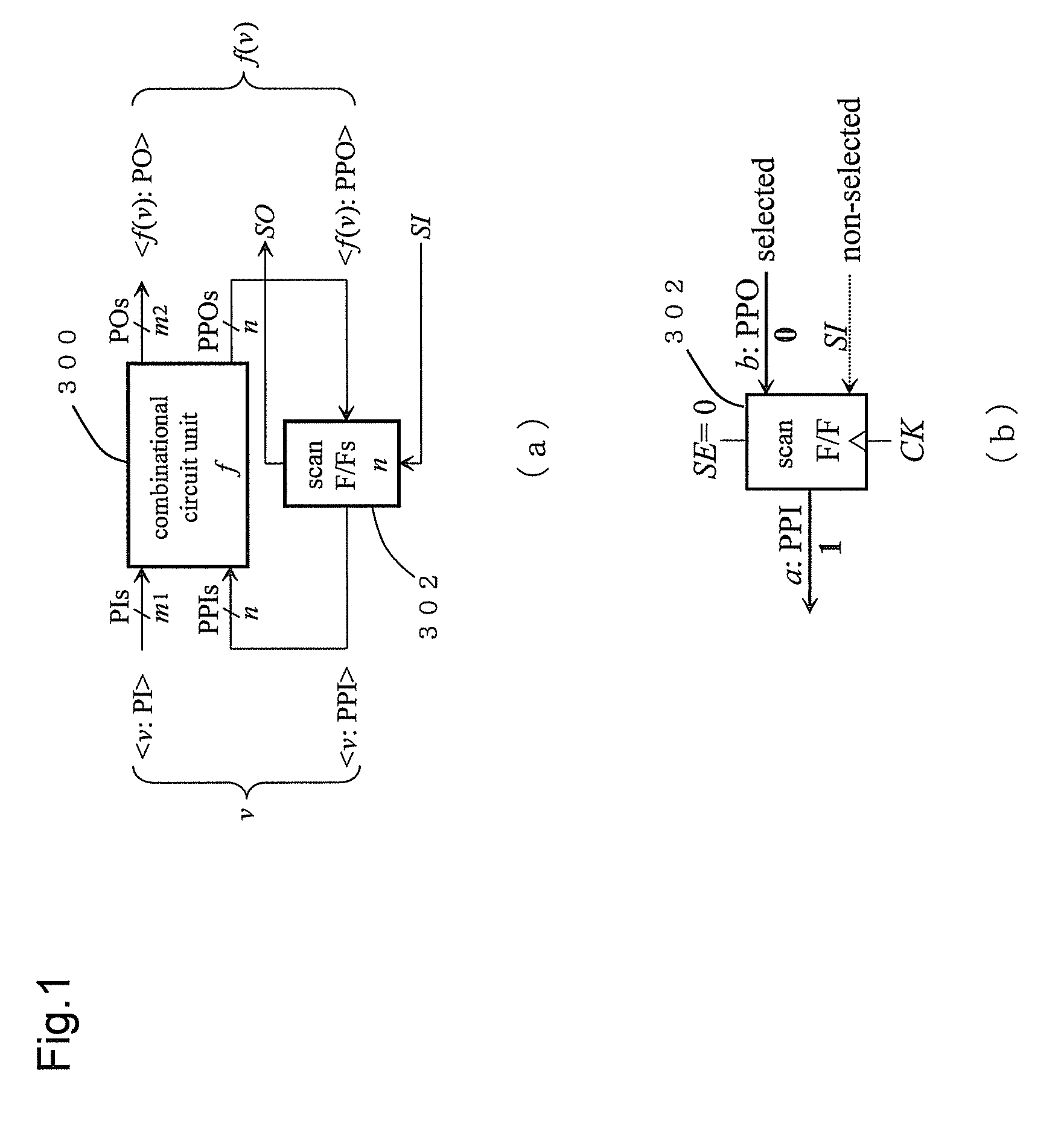
[0078]Referring to FIG. 1, a conventional full scan circuit, which is the background technology of the present invention, is described.

[0079]FIG. 1a) is a schematic diagram illustrating a constitution of the conventional full scan circuit. The full scan circuit comprises a combinational circuit unit 300 and a flip-flop 302 as a full scan sequential circuit. The combinational circuit unit 300 comprises an external input wire (PI), a pseudo external input wire (PPI) which is an output wire of the scan flip-flop, an external output wire (PO), and a pseudo external output wire (PPO) which is an input wire of the flip-flop. A part supplied directly from the external input wire and a part supplied via the pseudo external input wire constitute a test vector v for the combinational circuit unit 300. is set in the scan flip-flop 302 by the scan shift. An output from the combinational circuit unit 300 is a te...


PUM


Abstract

Provided are a conversion device and others for converting a test vector set so as to reduce a logic value difference generated before and after scan capture in outputs of scan cells included in a full scan sequential circuit. A conversion device 400 converts a test vector set corresponding to the full scan sequential circuit. The conversion device 400 comprises a setting unit 402 for setting a candidate bit which can be a don't care bit and a fixed bit which cannot be the don't care bit according to predetermined constraint conditions based on an input-output relationship in the logic circuit in order to identify the don't care bit identifiable as don't care from each test vector of the test vector set, and a logic value deciding unit 404 for deciding a logic value for the don't care bit in view of a relationship in a plurality of bit pairs in relation to a test cube including the don't care bit identified by the setting unit 402.

Description

CROSS-REFERENCE TO RELATED APPLICATIONS[0001]This application is a continuation-in-part of and claims the benefit of priority of co-pending PCT application Serial No. PCT / JP2006 / 323862 filed on Nov. 29, 2006, which in turn claims the benefit of priority of Japanese Patent Application No. 2005-346613 filed on Nov. 30, 2005, both of which are incorporated herein by reference.FIELD OF THE INVENTION[0002]The present invention relates to a conversion device, a conversion method, a program and a recording medium, more particularly to a conversion device and others for converting a test vector set for a logic circuit, and the like.BACKGROUND OF THE INVENTION[0003]As shown in FIG. 16, a semiconductor logic circuit is shipped through three stages, which are designing, manufacturing and testing stages. In the testing stage, a test vector, wherein the logic value of each logic bit is determined as either 0 or 1, is applied to the manufactured semiconductor logic circuit, and a test response fr...

Claims


Application Information

Patent Timeline
IPC IPC(8): G01R31/3177G06F11/25
CPCG01R31/318335G01R31/318547G01R31/318502
Inventor WEN, XIAOQINGKAJIHARA, SEIJIMIYASE, KOHEIMINAMOTO, YOSHIHIRODATE, HIROSHI
Owner JAPAN SCI & TECH CORP
Why Eureka
Try Eureka