Methods and heat treatment apparatus for uniformly heating a substrate during a bake process

a heat treatment apparatus and bake process technology, applied in the direction of electric heating for furnaces, furnace types, furnaces, etc., can solve the problems of difficult instantaneous determination of the temperature of the hotplate using a single temperature sensor, complicating the control of the resist feature dimensions, and unable to obtain the desired resist coating, etc., to achieve the effect of increasing the thermal conductivity

Active Publication Date: 2008-10-02
TOKYO ELECTRON LTD
View PDF51 Cites 11 Cited by
  • Summary
  • Abstract
  • Description
  • Claims
  • Application Information

AI Technical Summary

Benefits of technology

[0011]In an embodiment, a method for heating a substrate inside a processing chamber comprises supporting the substrate in a spaced relationship with a support surface in a first gas at approximately atmospheric pressure inside the processing chamber. The backside of the substrate is separated from the support surface by a heat exchange gap. The first gas is displaced from the heat exchange gap by a second gas having a higher thermal conductivity than the first gas to increase the thermal conductance between the substrate and the support surface. Heat energy is transferred from the support surface through the second gas in the heat exchange gap to the backside of the substrate for heating the substrate. As a result of the increased thermal conductivity, heat energy is conducted through the gap faster, minimizing temperature non-uniformity across the wafer and resulting in a more uniform heating of the wafer.

Problems solved by technology

When the wafer is treated with heat beyond the acceptable temperature range, a desired resist coating cannot be obtained.
Because the temperature of the entire hotplate is not uniform and varies with the lapsed time, however, it is difficult to instantaneously determine the temperature of the hotplate using a single temperature sensor.
First, the elevated temperature of the bake drives the diffusion of the photoproducts in the resist.
However, acid transport from nominally exposed to unexposed regions can complicate control of resist feature dimensions.
Acid transport through these reactive systems is mechanistically complex.
In addition to the intended results, numerous problems may be observed during heat treatment.
However, actual production wafers carrying deposited films on the surface of the silicon may exhibit small amounts of warpage because of the stresses induced by the deposited films.
Heat transfer through gases with low thermal conductivity, such as air, in the gap can cause temperature non-uniformity across the wafer surface as the temperature of the wafer is elevated to a process temperature.
This temperature non-uniformity may result in a change in critical dimension (CD) in that area of several nanometers, which can approach the entire CD variation budget for current leading edge devices, and will exceed the projected CD budget for smaller devices planned for production in the next few years.

Method used


Image

  • Methods and heat treatment apparatus for uniformly heating a substrate during a bake process
  • Methods and heat treatment apparatus for uniformly heating a substrate during a bake process
  • Methods and heat treatment apparatus for uniformly heating a substrate during a bake process

Examples


Embodiment Construction

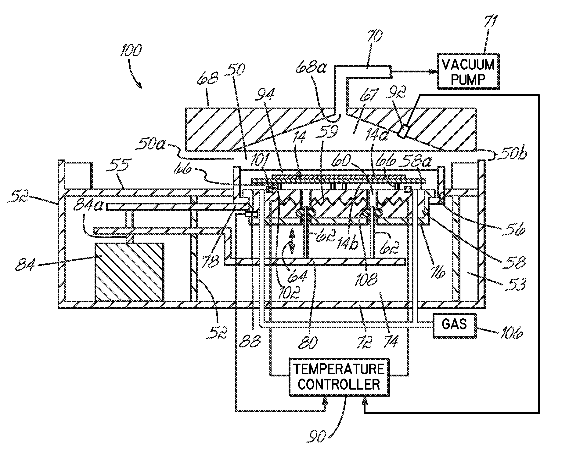
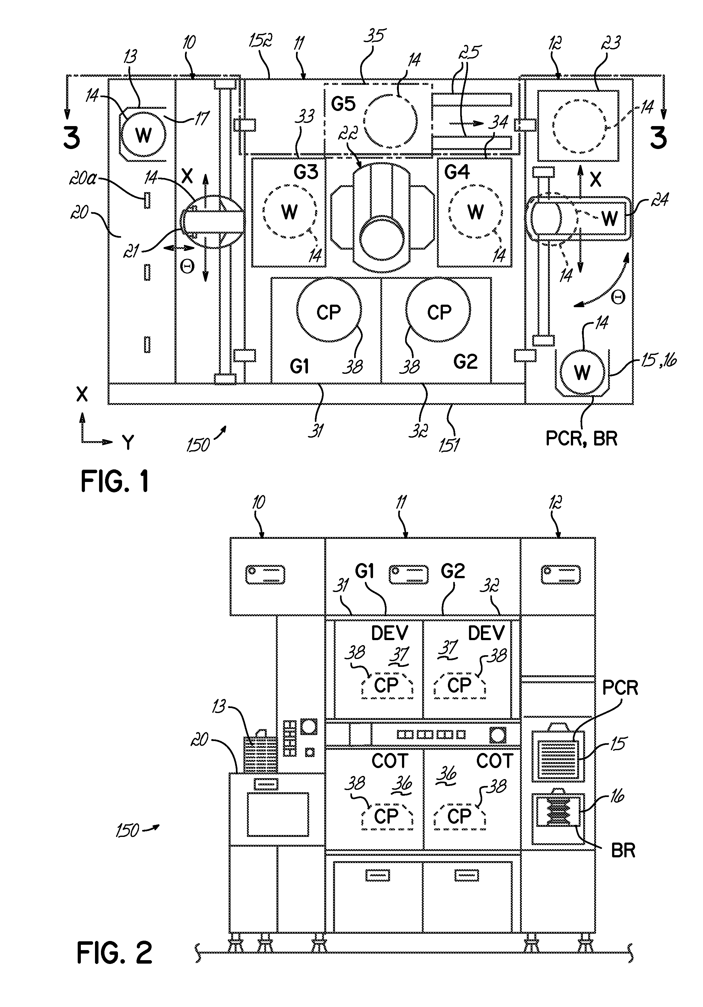
[0023]An embodiment of the method for thermally processing substrates utilizes the coating / developing process system 150. The substrate, generally in the form of a wafer composed of semiconducting material, is processed by the system 150. The processing is accomplished in such a way that the finished product will carry device structures on the top surface of the substrate.

[0024]With reference to FIGS. 1-3, the coating / developing process system 150 comprises a cassette station 10, a process station 11, and an interface section 12, which are contiguously formed as one unit. In the cassette station 10, a cassette (CR) 13 storing a plurality of substrates represented by wafers (W) 14 (e.g., 25 wafers) is loaded into, and unloaded from, the system 150. Each of the wafers 14 can be composed of a semiconductor material such as silicon, which may have the form of a single crystal material of the kind used in the art of semiconductor device manufacturing.

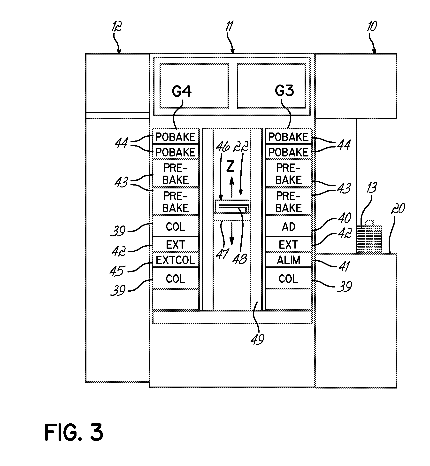
[0025]The process station 11 includes...


PUM

PropertyMeasurementUnit
temperatureaaaaaaaaaa
sizesaaaaaaaaaa
temperatureaaaaaaaaaa

Abstract

Methods and heat treatment apparatus for heating a substrate and any layer carried on the substrate during a bake process. A heat exchange gap between the substrate and a heated support is at least partially filled by a gas having a high thermal conductivity. The high thermal conductivity gas is introduced into the heat exchange gap by displacing a lower thermal conductivity originally present in the heat exchange gap when the substrate is loaded. Heat transfer across the heat exchange gap is mediated by the high thermal conductivity gas.

Description

FIELD OF THE INVENTION[0001]The invention relates to methods and heat treatment apparatus for thermally processing substrates, such as semiconductor wafers.BACKGROUND OF THE INVENTION[0002]Photolithography processes for manufacturing semiconductor devices and liquid crystal displays (LCD's) generally coat a resist on a substrate, expose the resist coating to light to impart a latent image pattern, and develop the exposed resist coating to transform the latent image pattern into a final image pattern having masked and unmasked areas. Such a series of processing stages is typically carried out in a coating / developing system having discrete heating sections, such as a pre-baking unit and a post-baking unit. Each heating section of the coating / developing system may incorporate a hotplate with a built-in heater of, for example, a resistance heating type.[0003]Feature sizes of semiconductor device circuits have been scaled to less than 0.1 micron. Typically, the pattern wiring that interc...

Claims


Application Information

Patent Timeline
Patent Type & Authority Applications(United States)
IPC IPC(8): F27D11/00
CPCF27B17/0025
Inventor SCHEER, STEVENCARCASI, MICHAEL A.
Owner TOKYO ELECTRON LTD
Why Eureka
Try Eureka