Method of Fabricating Back-Illuminated Imaging Sensors Using a Bump Bonding Technique

a technology of bump bonding and imaging sensors, which is applied in the direction of semiconductor devices, semiconductor/solid-state device details, electrical apparatus, etc., can solve the problems of front side illumination, imagers with significant performance limitations, low fill factor/low sensitivity, etc., and achieve the effect of reducing the overall siz

Inactive Publication Date: 2008-10-02
SRI INTERNATIONAL
View PDF4 Cites 16 Cited by
  • Summary
  • Abstract
  • Description
  • Claims
  • Application Information

AI Technical Summary

Problems solved by technology

Front side illumination, while traditionally utilized in standard imagers, has significant performance limitations such as low fill factor / low sensitivity.
The problem of low fill factor / low sensitivity is typically due to shadowing caused by the presence of opaque metal bus lines, and absorption by the array circuitry structure formed on the front surface in the pixel region.
It is also desirable to minimize the recombination of the generated carriers before they reach the front side, since such recombination reduces overall efficiency and sensitivity of the device.
This requires additional treatment at the backside of the device, which adds to the complexity of the fabrication process.
These methods can not be easily included in conventional semiconductor foundry processing, and require more expensive custom processing.
Fabrication of thinned back-illuminated imagers has other challenges: For example, thinned back illuminated imagers can have inherent dangling bonds present at the silicon back surface, which may cause generated electrons to recombine at the back surface.
Thinning of wafers poses yield issues such as stress in the thinned wafer due to non-uniformity of epitaxial layer thickness.
For these and the above reasons, fabrication cost is much higher for high volume production of back-illuminated imagers than for front illuminated imagers.
Fabrication of color filters and micro-lens for thinned back illuminated imagers, even for the method proposed above, is a complex process.
Back to front alignment is possible, but with less degree of alignment accuracy.
Apart from that, wire bonding and packaging of such back thinned imagers with color filters and micro-lenses add to complexity of the process.

Method used


Image

  • Method of Fabricating Back-Illuminated Imaging Sensors Using a Bump Bonding Technique
  • Method of Fabricating Back-Illuminated Imaging Sensors Using a Bump Bonding Technique
  • Method of Fabricating Back-Illuminated Imaging Sensors Using a Bump Bonding Technique

Examples


Embodiment Construction

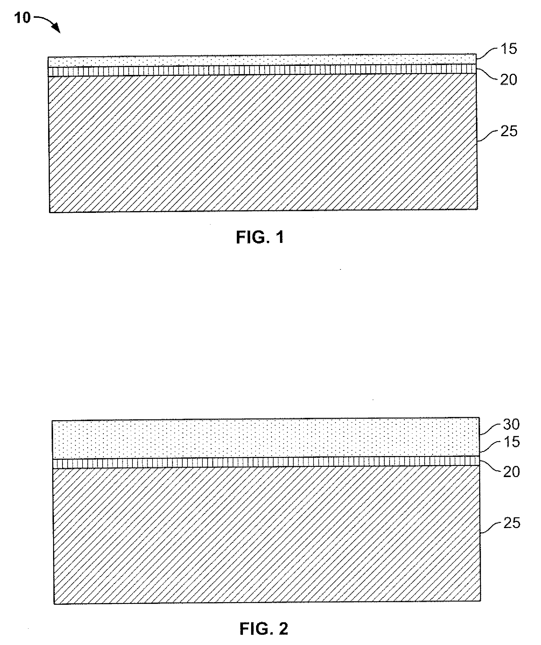
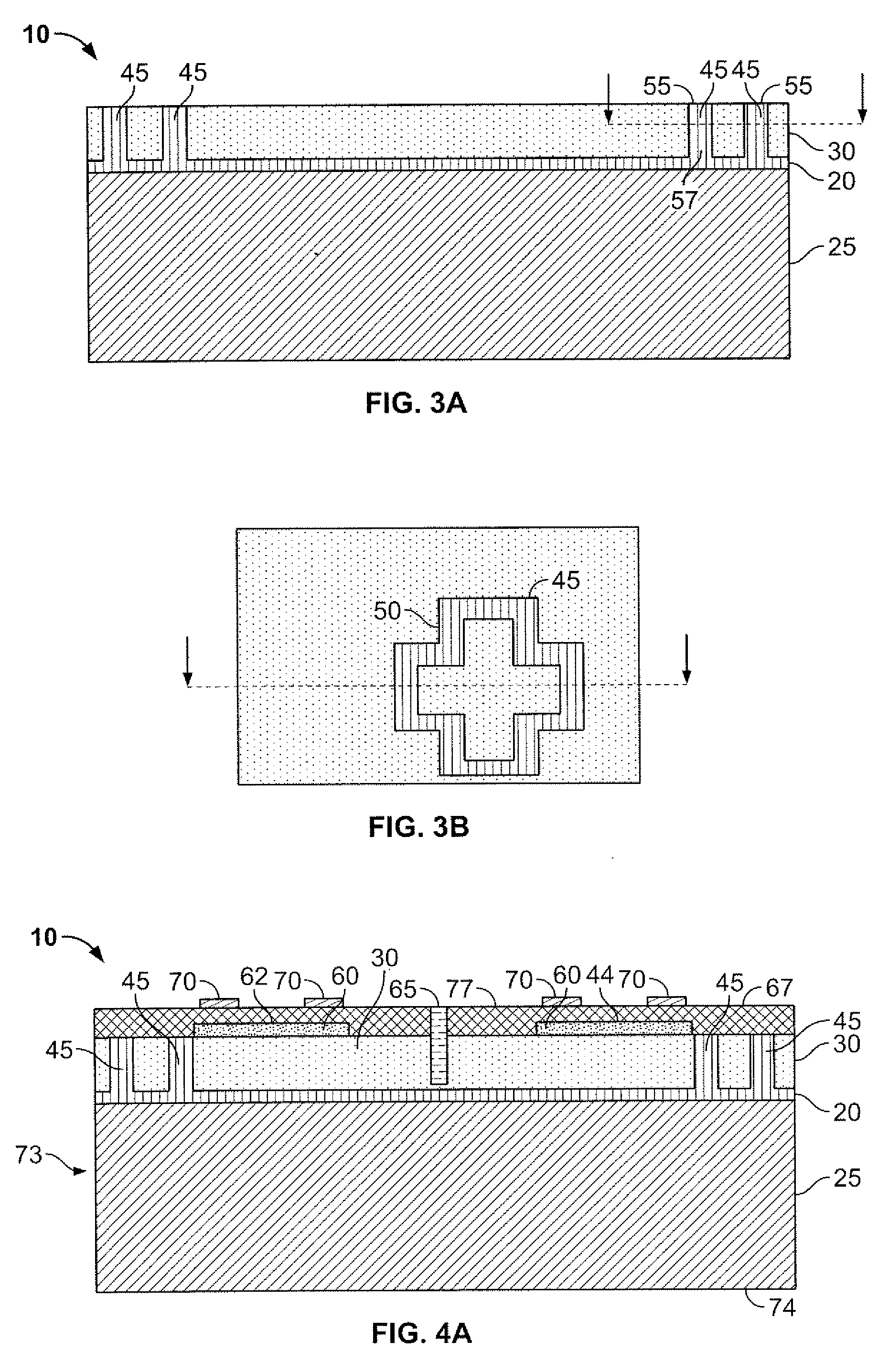
[0039]The following embodiments are intended as exemplary, and not limiting. In keeping with common practice, figures are not necessarily drawn to scale.

[0040]FIG. 1-15 illustrate an embodiment of a process for manufacturing thinned back-illuminated imagers and a resulting structure. FIG. 1 illustrates initial substrate 10 sometimes referred to in the art as a semiconductor-on-insulator (SOI) substrate. Starting SOI substrate 10, shown in FIG. 1, is composed of handle wafer 25 to provide mechanical support during processing, an insulator layer 20 (which can be, for example, a buried oxide layer of silicon), and seed layer 15. In the present embodiment, the handle wafer 25 may be a standard silicon wafer used in fabricating integrated circuits. Alternatively, the handle wafer 25 may be any sufficiently rigid substrate composed of a material which is compatible with the steps of the method disclosed herein. Insulator layer 20 may comprise an oxide of silicon with a thickness of about ...


PUM


Abstract

A method for fabricating a back-illuminated semiconductor imaging device on a semiconductor-on-insulator substrate, and resulting imaging device is disclosed. The method for manufacturing the imaging device includes the steps of providing a substrate comprising an insulator layer, and an epitaxial layer substantially overlying the insulator layer; fabricating at least one imaging component at least partially overlying and extending into the epitaxial layer; forming a plurality of bond pads substantially overlying the epitaxial layer; fabricating a dielectric layer substantially overlying the epitaxial layer and the at least one imaging component; providing a handle wafer; forming a plurality of conductive trenches in the handle wafer; forming a plurality of conductive bumps on a first surface of the handle wafer substantially underlying the conductive trenches; and bonding the plurality of conductive bumps to the plurality of bond pads.

Description

CROSS-REFERENCE TO RELATED APPLICATIONS[0001]This application claims the benefit of U.S. provisional patent application No. 60 / 908,436 filed Mar. 28, 2007, the disclosure of which is incorporated herein by reference in its entirety.FIELD OF THE INVENTION[0002]The field of the present invention is semiconductor device fabrication and device structure. More specifically, the present invention relates to a back illuminated image array device and a method of constructing such a device.BACKGROUND OF THE INVENTION[0003]CMOS or CCD image sensors are of interest in a wide variety of sensing and imaging applications in a wide range of fields including consumer, commercial, industrial, and space electronics. Imagers based on charge coupled devices (CCDs) are currently the most widely utilized. CCDs are employed either in front or back illuminated configurations. Front illuminated CCD imagers are cost effective to manufacture compared to back illuminated CCD imagers such that front illuminated...

Claims


Application Information

Patent Timeline
Patent Type & Authority Applications(United States)
IPC IPC(8): H01L31/0232H01L31/18
CPCH01L23/481H01L27/14618H01L27/14627H01L27/14683H01L2224/0557H01L27/1464H01L2224/13109H01L2224/13023H01L2924/0002H01L2224/0401H01L2924/1305H01L2924/00014H01L2924/00H01L2224/05552
Inventor SWAIN, PRADYUMNA KUMARLEVINE, PETERBHASKARAN, MAHALINGAMGOLDSMITH, NORMAN
Owner SRI INTERNATIONAL
Why Eureka
Try Eureka