
Tape carrier, semiconductor device, and method for manufacturing semiconductor device

a semiconductor device and tape carrier technology, applied in the direction of resist details, printed circuit aspects, non-metallic protective coating applications, etc., can solve the problems of color irregularities, uneven film thickness, defect in outer appearance, etc., and achieve the effect of less resistance, easy bending, and improved outer appearan

Inactive Publication Date: 2008-10-02
SEIKO EPSON CORP
View PDF5 Cites 2 Cited by
  • Summary
  • Abstract
  • Description
  • Claims
  • Application Information

AI Technical Summary

Benefits of technology

[0010]According to a first advantage of the invention, a tape carrier includes a base film with insulating property; a wiring pattern provided on the base film within a product region, the product region being demarcated by a cutting line so as to divide the tape carrier into individual products by cutting the tape carrier along the cut line; and a solder resist provided on the base film so as to cover the wiring pattern. The solder resist protrudes outward from within the product region.
[0011]With this structure, the tape carrier can be bended easily with less resistance, by arranging the bending line which is the bending axis so as to cover “a portion protruding outward from inside the product region” of the solder resist in plan view, at the time of bending and packaging the tape carrier into a case of an electric product after the tape carrier is divided into individual products. Moreover, compared to the common tape carrier, there are less thick film portions in the solder resist, improving the outer appearance.
[0012]In this case, the product region includes a bendable region having a bending line as an axis; and the solder resist is formed to protrude outward from within the product region, so as to overlap with the bending line in plan view,
[0013]With this structure, the core (i.e. the thick film portion of the solder resist) which is resistant to the bending of the tape carrier after cutting the tape carrier is made smaller or is not present. Therefore, the tape carrier is bended easily. Moreover, this improves the uniformity in the film thickness of the solder resists in the product region, thereby also improving the evenness in a stress distribution of the solder resists during the bending. Consequently, fluctuation in the manner of bending the tape carrier is reduced.
[0014]In this case, an edge of the solder resist is pulled out to the outside of the product region so that a thick film portion of the solder resist overlapping with the bending line in plan view is present only on the outside of the product region, and not on the cutting line nor inside the product region.
[0015]With this structure, when bending a tape carrier after dividing it, the core part (i.e. the thick film portion of the solder resist) which becomes resistant to bending is eliminated almost completely. Therefore, the tape carrier is bended easily enough, and the fluctuation in the manner of bending the tape carrier is sufficiently reduced.

Problems solved by technology

In other words, as shown in FIG. 4B, a part in each of the solder resists 205, positioned inward from the edge thereof by approximately 0.5 to 0.8 mm, is thicker compared to the center part, resulting in a problem of unevenness in film thickness.
Since the solder resists 205 are translucent, the uneven film thickness tends to cause color irregularities, i.e., defect in the outer appearance.
This results in the irregularities of bending, i.e., defect in bending.

Method used


Image

  • Tape carrier, semiconductor device, and method for manufacturing semiconductor device
  • Tape carrier, semiconductor device, and method for manufacturing semiconductor device
  • Tape carrier, semiconductor device, and method for manufacturing semiconductor device

Examples


Embodiment Construction

[0029]Embodiments of the invention will now be described with references to the accompanying drawings.

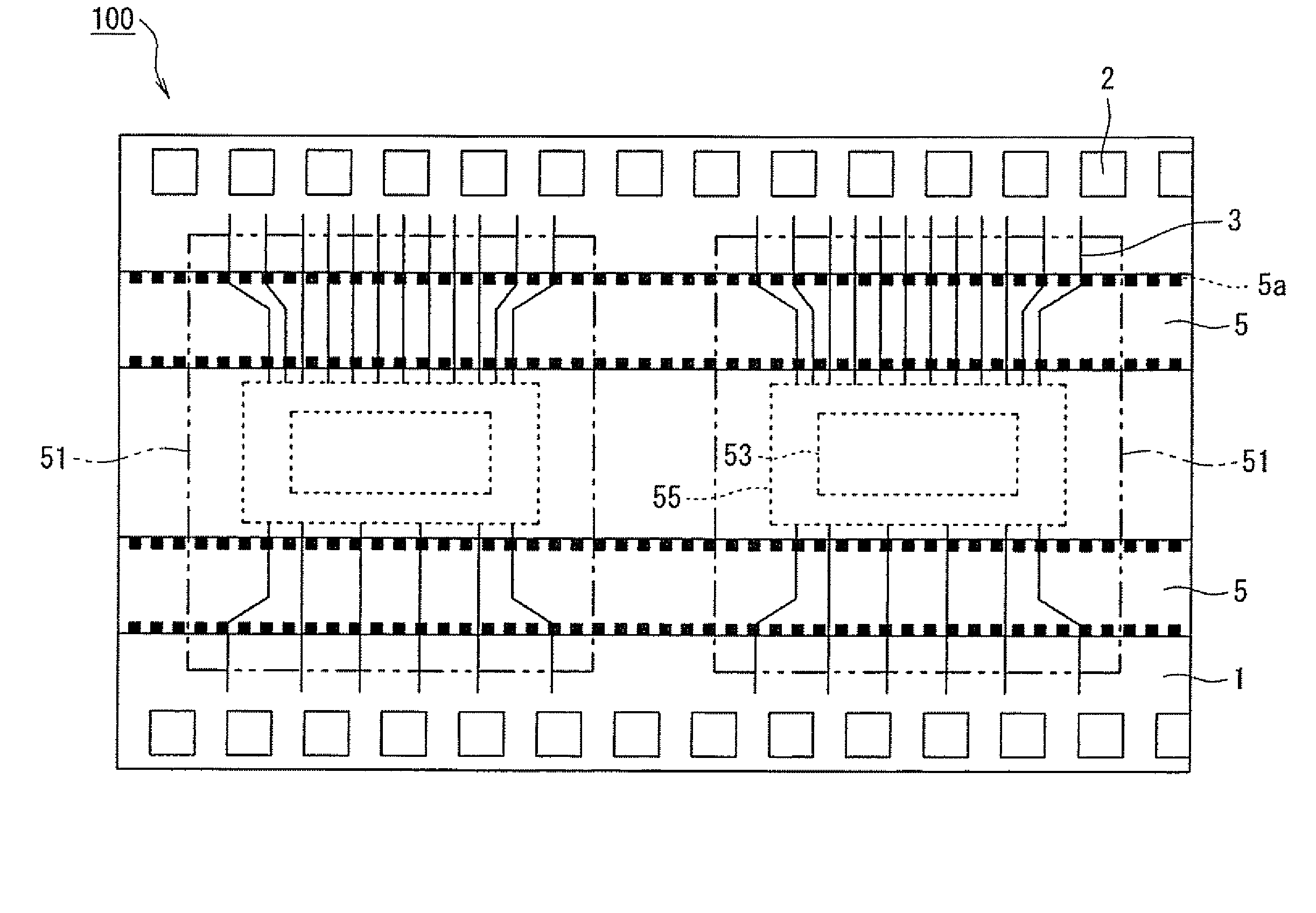
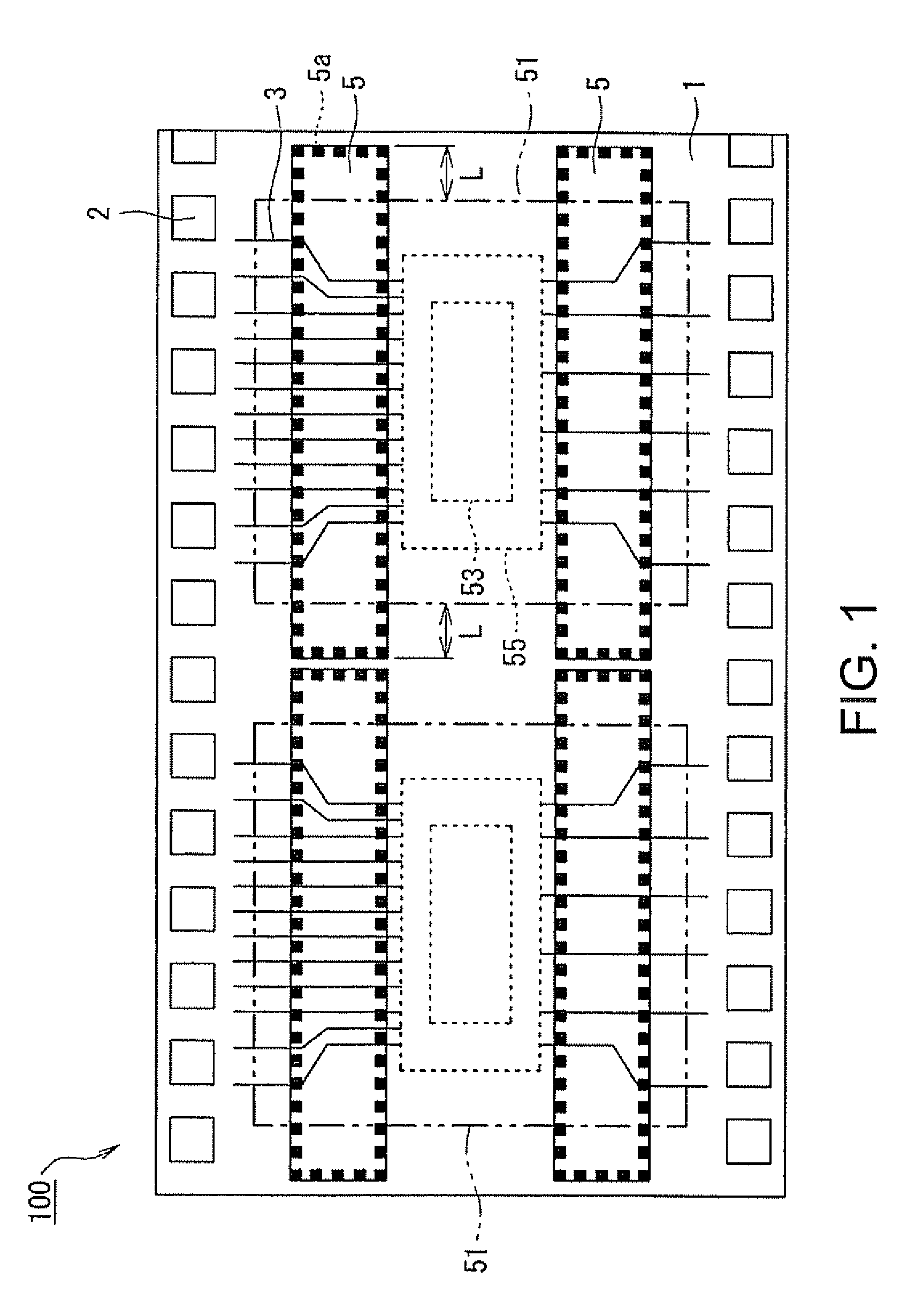
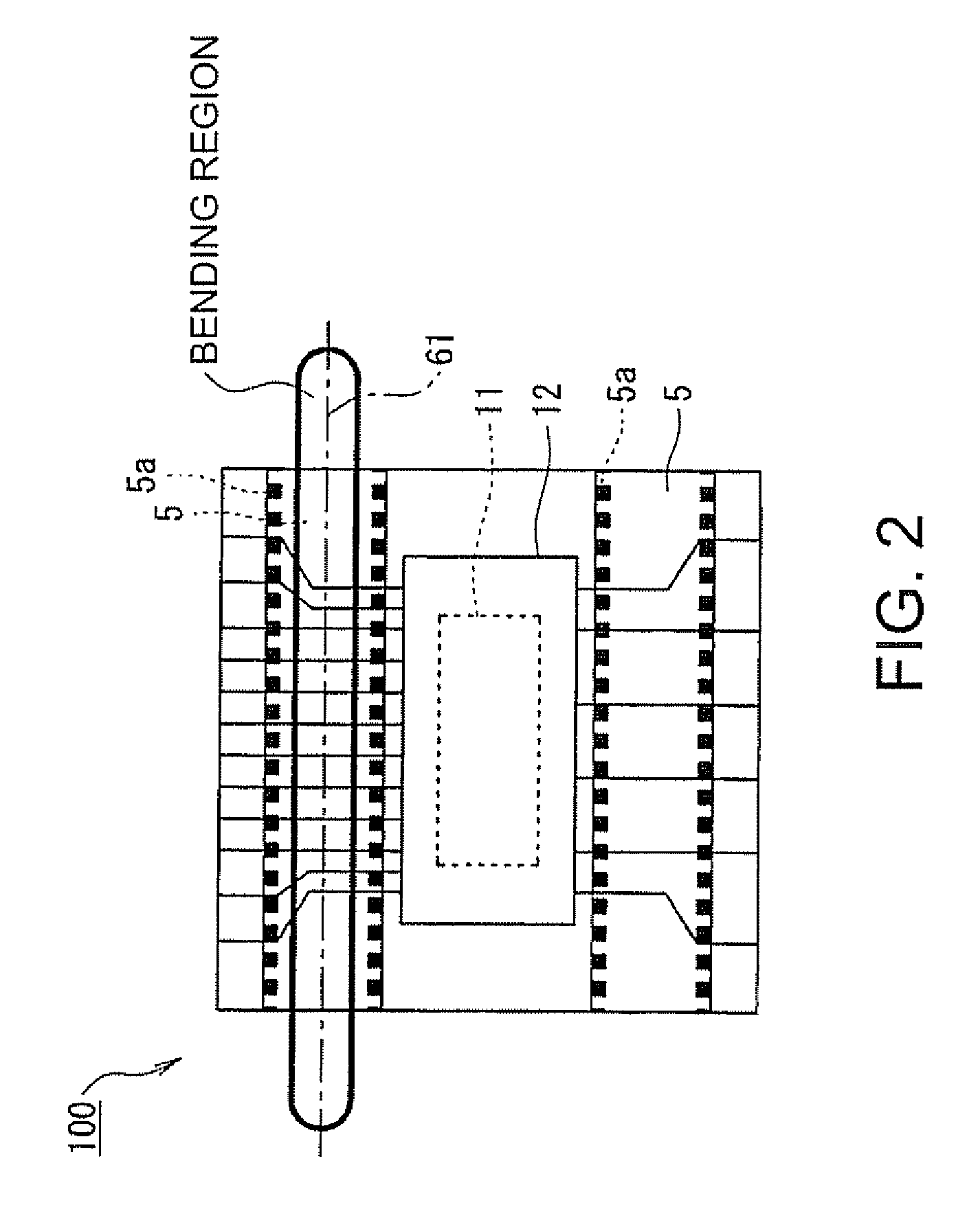
[0030]FIGS. 1 and 2 are plan views illustrating an example of a structure of a tape carrier 100 according to one embodiment of the invention. Specifically,FIG. 1 indicates a state of the tape carrier 100 before stamping the tape carrier along cut lines 51 that demarcate a production region. The double dotted lines in FIG. 1 are the cut lines 51 and regions surrounded thereby are product regions. Moreover, FIG. 2 indicates the tape carrier 100 divided into individual products by stamping the tape carrier 100 along the cut lines 51.

[0031]As shown in FIG. 1, the tape carrier 100 includes, in a state prior to being stamped, a long base film 1, sprocket holes 2 provided on a side edge in the longitudinal direction of the base film 1, inner and outer leads (hereafter referred to as “leads”) 3, and solder resists 5 coated on the tape carrier 100 so as to cover these leads 3. The base film ...


PUM


Abstract

A tape carrier includes: a base film with insulating property; a wiring pattern provided on the base film within a product region, the product region being demarcated by a cutting line so as to divide the tape carrier into individual products by cutting along the tape carrier along the cut line; and a solder resist provided on the base film so as to cover the wiring pattern. The solder resist protrudes outward from within the product region.

Description

[0001]The entire disclosure of Japanese Patent Application No. 2007-088237, filed Mar. 29, 2007 is expressly incorporated by reference herein.BACKGROUND[0002]1. Technical Field[0003]The present invention relates to a tape carrier, a semiconductor device, and a method for manufacturing semiconductor device.[0004]2. Related Art[0005]Size and weight reduction of electric products such as liquid crystal panels and mobile terminals is advancing. These electric products include integrated circuit devices, and these devices packaged inside cases are generally mounted on insulating film substrates that can be bended easily, for instance, by hand. These film substrates are formed with, for instance, polyimide, and are called tape carriers or flexible substrates. Packaged products including integrated circuit devices mounted on such tape carriers are called tape carrier packages (TCP), chip on films (COF), or flexible print circuits (FPC). Refer to JP-A-2004-235322 and JP-A-2000-269249 for ex...

Claims


Application Information

Patent Timeline
Patent Type & Authority Applications(United States)
IPC IPC(8): H01L23/495H01L21/00
CPCH01L23/4985H05K1/028H05K3/28H05K2201/09909H05K2201/10681H01L2924/0002H05K2203/0594H01L2924/00
Inventor YANAGISAWA, MASAHIKO
Owner SEIKO EPSON CORP
Learn More