Integrated circuit with flexible planer leads

Active Publication Date: 2008-10-02
MICROSEMI
View PDF14 Cites 8 Cited by
  • Summary
  • Abstract
  • Description
  • Claims
  • Application Information

AI Technical Summary

Benefits of technology

[0008]The present invention achieves technical advantages as a microelectronic device including a microelectronic circuit and a planar flexible lead. The planar flexible lead is adapted to bend and flex during mechanical stress and during extreme temperature cycling, and allow direct mounting of the device to a member by easily welding or soldering.

Problems solved by technology

These solar cell diodes are subject to some of the most severe thermal cycling environments given their exposure to the sun and subsequent shading therefrom numerous times over their life cycle.
These rigid leads can tolerate the extreme thermal cycling for a period of time, but have a limited life cycle.
The solder joint in this design has limited thermal cycling capability due to thermal expansion mismatch, solder re-crystallization, and solder creep.
The axial leads do not lend themselves to welding easily.
Solar panel manufactures struggle with the weld attachment.
Welding flat leads to round axial leads causes reliability and weld consistency problems.
Integrated circuits generate heat during operation due to conduction losses.
Axial leaded glass diodes in particular are very difficult to heat sink to the panel and remove the heat efficiently.
Solar panel manufactures have been struggling with thermal problems associated with the axial leaded glass diodes.

Method used


Image

  • Integrated circuit with flexible planer leads
  • Integrated circuit with flexible planer leads
  • Integrated circuit with flexible planer leads

Examples


Embodiment Construction

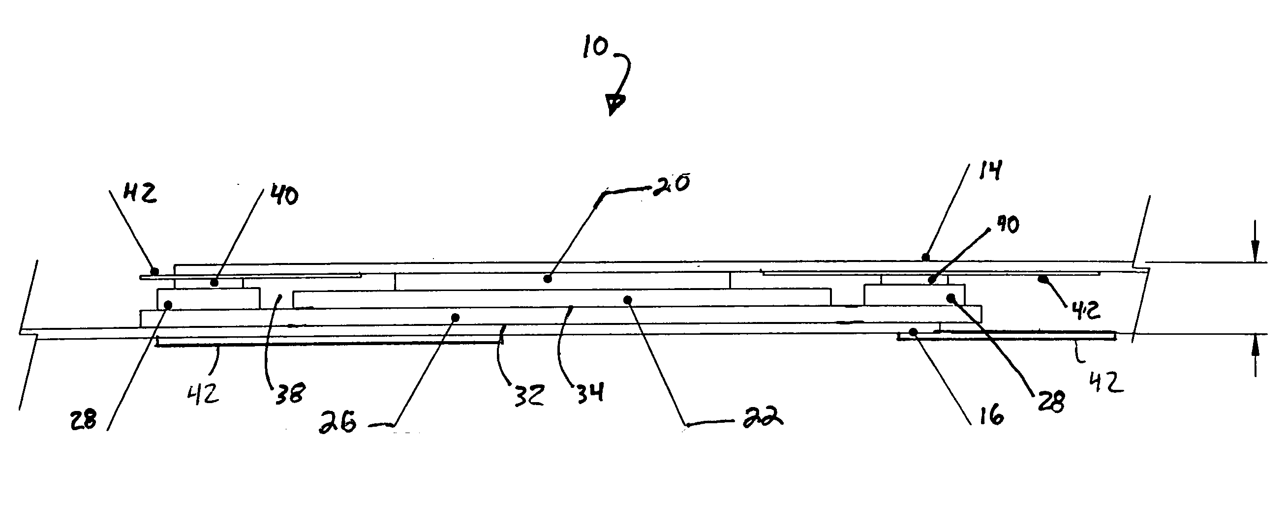
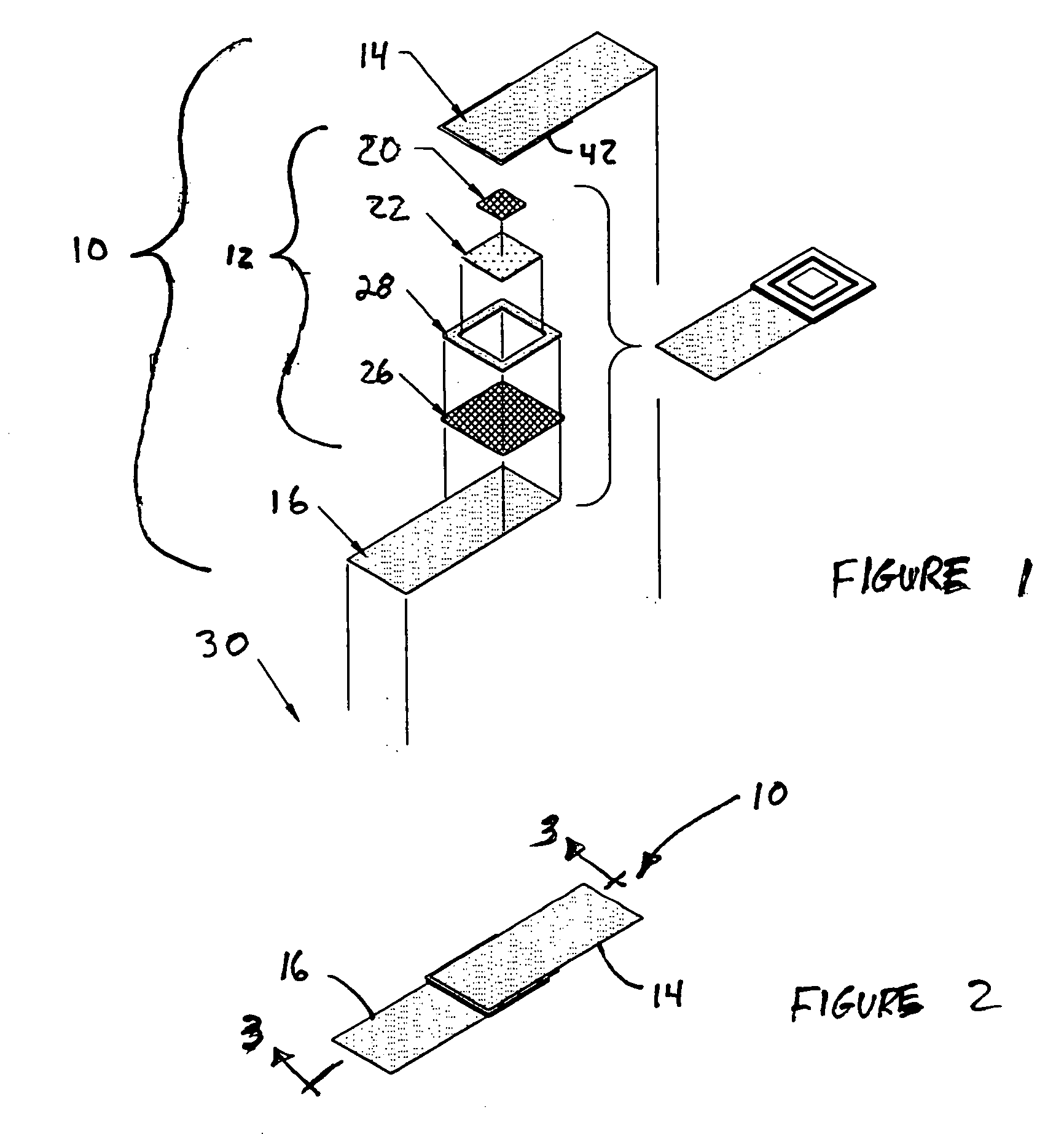
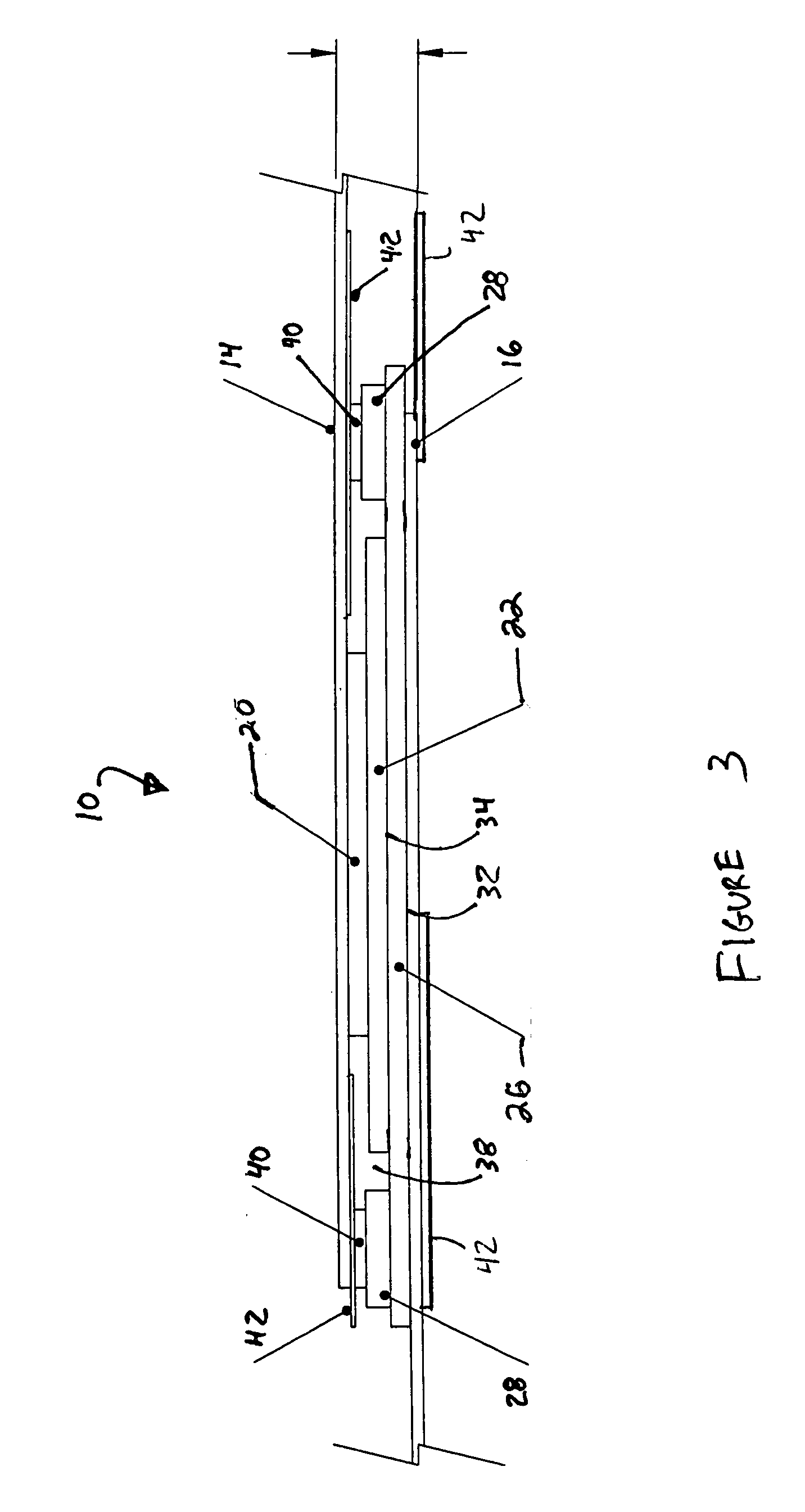
[0015]Referring to FIG. 1, there is generally shown at 10 a microelectronic device seen to include an integrated circuit assembly 12 interposed between a pair of planar flexible leads 14 and 16. The integrated circuit assembly 12 is seen to comprise a microelectronic circuit 22, such as a die, disposed upon a moly substrate 26, which substrate 26 is secured upon the flex lead 16, as shown. A ring 28 is formed upon the substrate 26, and forms a die attach cavity 38 configured to receive the microelectronic, (FIG. 3).

[0016]Advantageously, the planar flexible leads 14 and 16 are each formed as a thin sheet such as they are configured to flex, particularly during mechanical stress and during extreme thermal cycling. The planar flexible leads 14 and 16 may be formed as a membrane, but may have other shapes and profiles, and have an electrically conductive portion permitting electrical signals to pass from the die 22 to another member coupled to the respective flexible lead 14 or 16. Acco...


PUM


Abstract

A microelectronic device including a microelectronic circuit and at least one planar flexible lead. These planar flexible leads are adapted to bend and flex during mechanical stress allow direct mounting of the device to a member, and withstand extreme thermal cycling, such as −197° C. to +150° C. such as encountered in space.

Description

PRIORITY CLAIM[0001]This application claims priority of U.S. Provisional Ser. No. TBD, Attorney Docket No. A1147 SD entitled “Integrated Circuit with Flexible Planer Leads” filed Mar. 23, 2007.FIELD OF THE INVENTION[0002]The present invention is generally directed to integrated circuits, and more particularly to integrated circuit packages including diodes that are adapted to withstand extreme thermal cycling, such as that incurred in a space environment, such as solar panels.BACKGROUND OF THE INVENTION[0003]Microelectronic devices typically comprise of an integrated circuit diode die encompassed in a package having a plurality of external leads permitting electrical attachment to a printed circuit board. These microelectronic devices are available as commercial devices, and some are available as high reliability devices such as used in military applications, including those integrated in space environments, such as satellites, space vehicles and solar panels. In space environments,...

Claims


Application Information

Patent Timeline
IPC IPC(8): H01L23/48
CPCH01L23/047H01L23/051H01L23/057H01L23/4985H01L31/02008H01L31/042H01L2224/73253H01L2924/01079H01L2924/14Y02E10/50H01L31/048H01L31/02005H01L2924/12032H01L31/044H01L2924/00H01L23/498
Inventor AUTRY, TRACY
Owner MICROSEMI
Why Eureka
Try Eureka