Semiconductor memory device

Inactive Publication Date: 2008-10-02
LONGITUDE SEMICON S A R L
View PDF4 Cites 4 Cited by
  • Summary
  • Abstract
  • Description
  • Claims
  • Application Information

AI Technical Summary

Benefits of technology

[0011]That is, an object of the invention is to provide a control signal generator that not only adjusts the operation cycle time of one control signal to column cycle time but adjusts operating time difference among plural control signals to the column cycle time.

Problems solved by technology

However, in this method of generating timing in a column cycle using the access time, the following problem occurs.
Conversely, as a chip with bad performance is operated at the similar rate to 667 MHz though the chip is to be operated at the clock frequency of 533 MHz when a clock frequency is set to 667 MHz, a problem that the operational margin is deteriorated occurs.

Method used


Image

  • Semiconductor memory device
  • Semiconductor memory device
  • Semiconductor memory device

Examples


Embodiment Construction

[0042]Referring to the drawings, embodiments of the invention will be described in detail below.

[0043]A circuit element forming each block in the embodiments is not particularly limited, however, the circuit element is formed on one semiconductor substrate made of monocrystalline silicon and others. A metal oxide semiconductor field effect transistor (MOSFET) without an arrow denotes N-type MOSFET (NMOSFET) and is distinguished from P-type MOSFET (PMOSFET) with an arrow. The MOSFET will be briefly called MOS below. However, the invention is not limited to only a field effect transistor including an oxide insulating film provided between a metal gate and a semiconductor layer and is applied to a circuit using general FET such as a metal insulator semiconductor field effect transistor (MISFET).

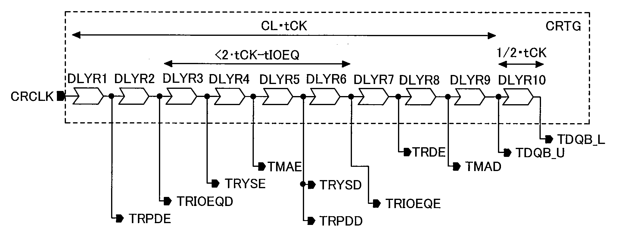
[0044]FIG. 1 shows the embodiment of the invention. FIG. 1 shows an example of the configuration of a timing control circuit for controlling the timing of column operation in a read command for ...


PUM


Abstract

The semiconductor memory device according to the invention is provided with a first delay circuit block that generates a timing signal of a circuit block to be operated in column cycle time determined by an external input command cycle and a second delay circuit block the whole delay of which is controlled to be a difference between access time determined by an external clock and the latency and column cycle time. These delay circuit blocks are controlled so that the delay of each delay circuit is a suitable value in accordance with column latency and an operating frequency, and each delay is controlled corresponding to dispersion in a process and operating voltage and a change of operating temperature.

Description

CLAIM OF PRIORITY[0001]The present application claims priority from Japanese application JP 2007-088693, filed on Mar. 29, 2007, the content of which is hereby incorporated by reference into this application.BACKGROUND OF THE INVENTION[0002]1. Field of the Invention[0003]The present invention relates to a semiconductor memory device, particularly relates to a control signal generator of a memory array for realizing stable operation at different external clock frequencies.[0004]2. Description of the Related Arts[0005]Synchronous DRAM (SDRAM) realizes a high-speed data rate by inputting and outputting a command and data in synchronization with an external clock. Recently, double data rate (DDR) SDRAM, DDR2 SDRAM and DDR3 SDRAM that respectively realize a further higher-speed data rate are developed. Of these DRAMs, a column command (read / write) can be input to SDRAM and DDR SDRAM every clock cycle from an external device. In DDR2 SDRAM, it can be input every two clocks and in DDR3 SDR...

Claims


Application Information

Patent Timeline
IPC IPC(8): G11C8/00G06F1/06G11C11/407G11C11/4076H03K5/13
CPCG11C7/04G11C7/1066G11C7/1072G11C7/22G11C7/222G11C11/4076G11C2207/2272G11C11/407
Inventor TAKEMURA, RIICHIROSEKIGUCHI, TOMONORIAKIYAMA, SATORUNAKAYA, HIROAKINAKAMURA, MASAYUKI
Owner LONGITUDE SEMICON S A R L
Why Eureka
Try Eureka