Optoelectronic device and method of fabricating the same

a technology of optoelectronic devices and fabrication methods, applied in the field of optoelectronic devices and methods of fabricating the same, can solve the problems of insufficient coverage, poor thickness control, and usually passivation layers, and achieve excellent surface passivation effect, enhance the performance and avoid the effect of destroying the prepared structure of the optoelectronic devi

Inactive Publication Date: 2008-10-02
CHEN MIIN JANG
View PDF6 Cites 55 Cited by
  • Summary
  • Abstract
  • Description
  • Claims
  • Application Information

AI Technical Summary

Benefits of technology

[0011]Therefore, according to the invention, the method of fabricating an optoelectronic device forms a passivation layer overlaying the multi-layer structure by an atomic layer deposition based process. Thereby, the passivation layer can provide excellent surface passivation effect, so as to enhance the performance of the optoelectronic device. Furthermore, since the processing temperature is relatively lo

Problems solved by technology

However, traditionally produced passivation layers usually have some flaws such as poor thickness control, insufficient coverage, or high defect density.
Such poor-quality passivation layers do not help a lot in improving the properties of the optoele

Method used


Image

  • Optoelectronic device and method of fabricating the same
  • Optoelectronic device and method of fabricating the same
  • Optoelectronic device and method of fabricating the same

Examples


Embodiment Construction

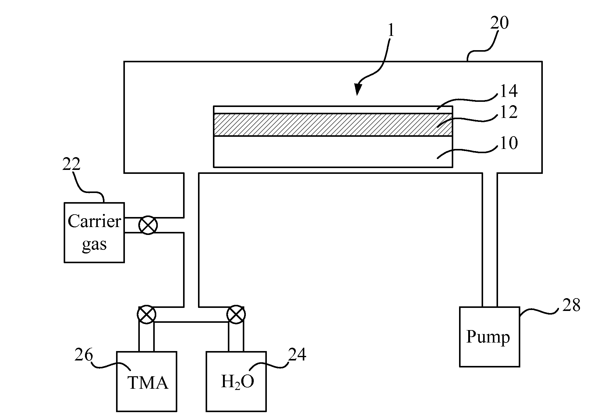
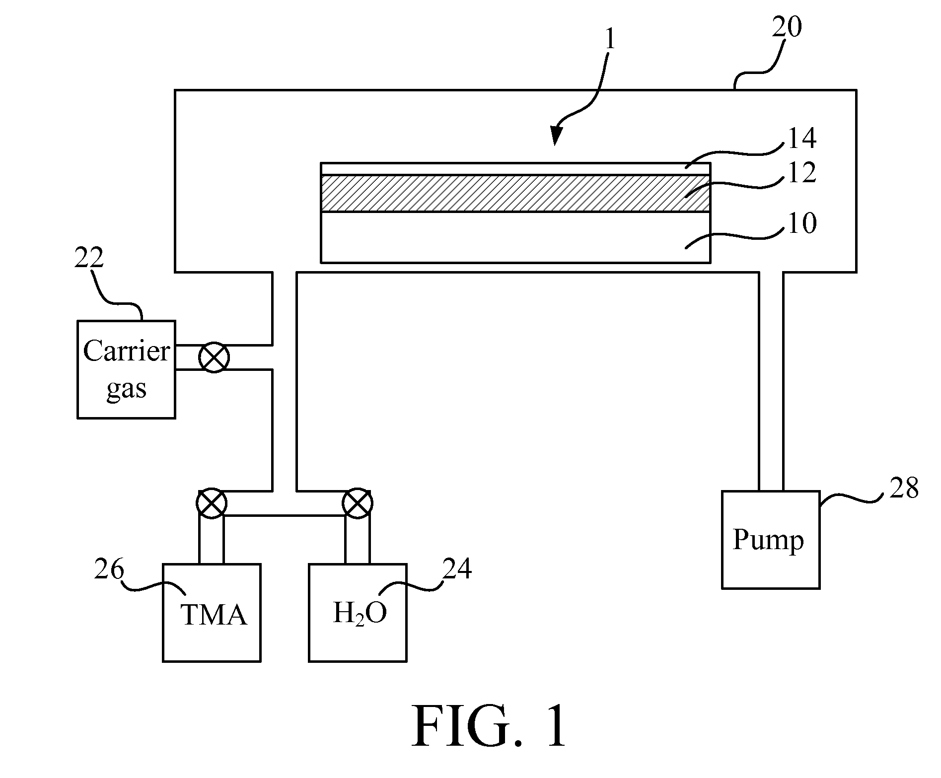
[0019]Please refer to FIG. 1. FIG. 1 shows the fabrication method according to an embodiment of the invention. The fabrication method according to an embodiment of the invention is used for fabricating an optoelectronic device 1. In actual applications, the optoelectronic device 1 can be an organic light-emitting diode, an organic solar cell, an inorganic light-emitting diode, an inorganic solar cell, a photo-detector, a laser diode, or the like.

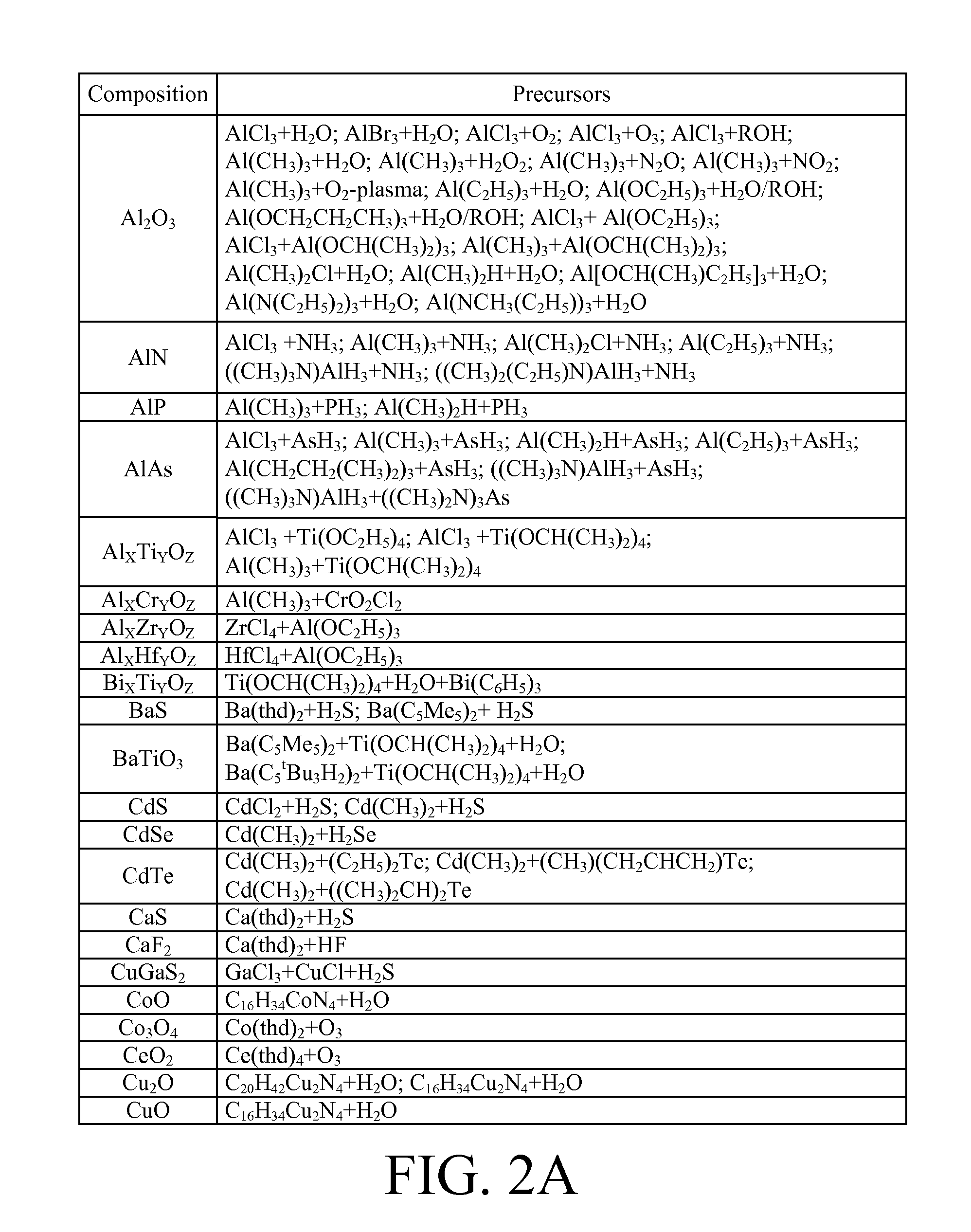
[0020]As shown in FIG. 1. The method, firstly, prepares a substrate 10. Then, the method forms a multi-layer structure 12 on the substrate 10. In the embodiment, the substrate 10 can be a sapphire substrate, a Si substrate, a SiC substrate, a GaN substrate, AlGaN substrate, a InGaN substrate, a ZnO substrate, a ScAlMgO4 substrate, a YSZ (yttria-stabilized zirconia) substrate, a SrCu2O2 substrate, a CuAlO2 substrate, LaCuOS substrate, a NiO substrate, a LiGaO2 substrate, a LiAlO2 substrate, a GaAs substrate, a InP substrate, a glass substrate...


PUM

PropertyMeasurementUnit
Temperatureaaaaaaaaaa

Abstract

The invention provides an optoelectronic device and the fabrication thereof. The method according to the invention, firstly, prepares a substrate. Then, the method forms a multi-layer structure on the substrate. Afterward, by an atomic layer deposition based process, the method forms a passivation layer overlaying the multi-layer structure.

Description

BACKGROUND OF THE INVENTION[0001]1. Field of the Invention[0002]The invention relates to an optoelectronic device and method of fabricating the same, and more particularly, to an optoelectronic device and fabrication method which forms a passivation layer by an atomic layer deposition based process.[0003]2. Description of the Prior Art[0004]Along with the rapid development of optoelectronic industry, versatile optoelectronic devices such as light-emitting diodes, laser diodes, photo-detectors, and solar cells, are extensively used in many fields of applications. Moreover, with the progress of the optoelectronic technologies, required performance of properties, such as light emission efficiency and optoelectronic conversion efficiency, are as well getting higher and higher.[0005]Generally speaking, forming a passivation layer on the surface of an optoelectronic device can improve, to some extent, some properties of the optoelectronic device, such as light emission efficiency and opto...

Claims


Application Information

Patent Timeline
IPC IPC(8): C23C16/513B05D5/12B32B9/04
CPCC23C16/45525H01L31/0216H01L33/44Y10T428/249921
Inventor CHEN, MIIN JANGSHIH, YING TSANG
Owner CHEN MIIN JANG
Why Eureka
Try Eureka