Solar cell with passivation contact and preparation method thereof

A solar cell and contact area technology, applied in the field of solar cells, can solve problems such as the large gap between cell efficiency and theoretical efficiency, lowering the power generation efficiency of solar cells, and decreasing current density, achieving good surface passivation effect and improving cell performance. , reduce the effect of surface recombination

Pending Publication Date: 2021-11-12
TRINA SOLAR CO LTD
View PDF3 Cites 4 Cited by
  • Summary
  • Abstract
  • Description
  • Claims
  • Application Information

AI Technical Summary

Problems solved by technology

[0008] In existing solar cells, after screen printing and sintering, the metal electrodes are in direct contact with the semiconductor body, resulting in a high recombination rate, which makes the current battery efficiency and theoretical efficiency still far behind.
At present, in order to solve the contact problem of metal electrodes, a whole-surface passivation layer doped with polysilicon is usually used to improve the electrode contact performance, but doped polysilicon has strong light absorption characteristics, so that part of the incident light cannot be effectively used by the battery, resulting in light Parasitic losses lead to a drop in current density, lowering solar cell power generation efficiency

Method used


Image

  • Solar cell with passivation contact and preparation method thereof
  • Solar cell with passivation contact and preparation method thereof
  • Solar cell with passivation contact and preparation method thereof

Examples


Embodiment 1

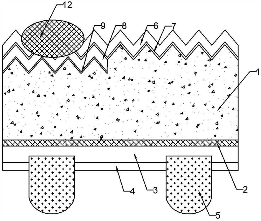
[0071] This embodiment provides a solar cell, the solar cell is as figure 1As shown, including the substrate 1, the metal contact region on the front side of the substrate 1 is sequentially stacked with a front tunnel oxide layer 9 (silicon oxide layer) and a front doped polysilicon layer 8 (phosphorous doped polysilicon layer), and the front tunnel oxide layer Layer 9 has a thickness of 2 nm, and the front doped polysilicon layer 8 has a thickness of 200 nm. The front doped polysilicon layer 8 and the surface of the non-metal contact region are sequentially stacked with a phosphorus diffusion layer-A (front surface field FSF) 7 and a front anti-reflection layer 6, and the thickness of the phosphorus diffusion layer-A (front surface field FSF) 7 is The thickness of the front anti-reflection layer 6 is 50 nm. Front metal grid lines 12 are formed on the surface of the front antireflection layer 6 , and the front metal grid lines 12 are in contact with the front doped polysilico...

Embodiment 2

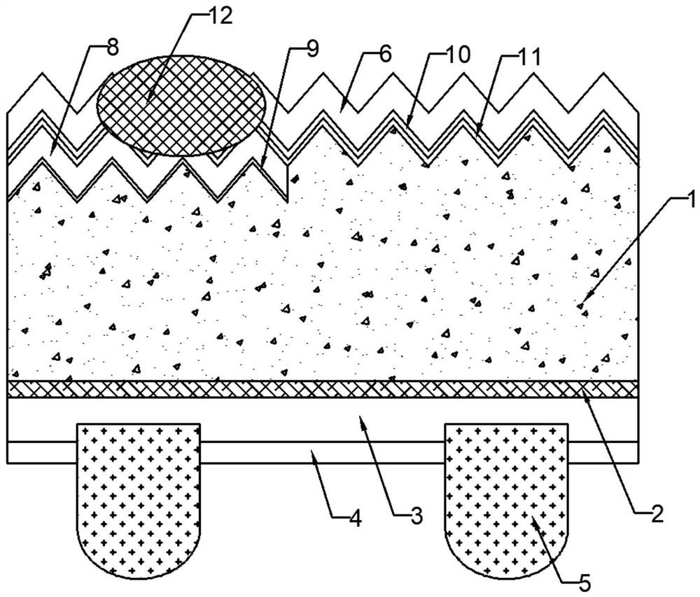
[0085] This embodiment provides a solar cell, the solar cell is as figure 2 As shown, including the substrate 1, the metal contact region on the front side of the substrate 1 is sequentially stacked with a front tunnel oxide layer 9 (silicon oxide layer) and a front doped polysilicon layer 8 (phosphorous doped polysilicon layer), and the front tunnel oxide layer Layer 9 has a thickness of 3nm and front doped polysilicon layer 8 has a thickness of 200nm. The front doped polysilicon layer 8 and the surface of the non-metal contact area are sequentially stacked with a phosphorus diffusion layer-B 11, an oxide layer 10, and a front anti-reflection layer 6. The thickness of the oxide layer 10 is 3 nm, and the thickness of the front anti-reflection layer 6 is 100 nm. . Front metal grid lines 12 are formed on the surface of the front antireflection layer 6 , and the front metal grid lines 12 are in contact with the front doped polysilicon layer 8 .

[0086] The back side of the su...

Embodiment 3

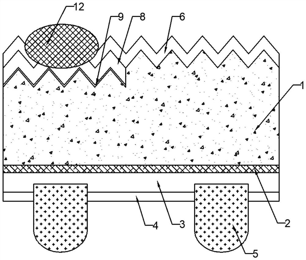
[0100] This embodiment provides a solar cell, the solar cell is as image 3 As shown, including the substrate 1, the metal contact region on the front side of the substrate 1 is sequentially stacked with a front tunnel oxide layer 9 (silicon oxide layer) and a front doped polysilicon layer 8 (phosphorous doped polysilicon layer), and the front tunnel oxide layer Layer 9 has a thickness of 2 nm, and the front doped polysilicon layer 8 has a thickness of 400 nm. The surface of the front doped polysilicon layer 8 and the non-metal contact area is provided with a front anti-reflection layer 6, and the thickness of the front anti-reflection layer 6 is 200nm. Front metal grid lines 12 are formed on the surface of the front antireflection layer 6 , and the front metal grid lines 12 are in contact with the front doped polysilicon layer 8 .

[0101] The back side of the substrate 1 is sequentially stacked with a back tunneling oxide layer 2 (silicon oxide layer), a back doped polysili...


PUM

PropertyMeasurementUnit
thicknessaaaaaaaaaa
thicknessaaaaaaaaaa
thicknessaaaaaaaaaa

Abstract

The invention provides a solar cell with passivation contact and a preparation method thereof. The solar cell comprises a substrate, a back tunneling oxide layer, a back passivation film and a back anti-reflection layer are sequentially arranged on the back face of the substrate in a stacked mode, a back metal grid line is formed on the surface of the back anti-reflection layer, and the back metal grid line is in contact with the back passivation film; the front surface of the substrate is divided into a metal contact region and a non-metal contact region, the metal contact region is sequentially provided with a front tunneling oxide layer, a front passivation film and a front anti-reflection layer in a stacked manner, and a front metal grid line is formed on the surface of the front anti-reflection layer and is in passivation contact with the front passivation film. According to the solar cell, the recombination of a metal-semiconductor interface in a contact region is effectively reduced, and the surface passivation performance is improved, so that the open-circuit voltage and the fill factor of the cell are greatly improved, and the cell performance is improved.

Description

technical field [0001] The invention belongs to the technical field of solar cells, and relates to a solar cell with a passivation contact and a preparation method thereof. Background technique [0002] Solar energy, as a renewable energy source, has received worldwide attention from the early days of its invention, and recently, since existing energy sources such as oil and coal are expected to be exhausted, interest in alternative energy sources for use in place of existing energy sources is growing, More and more solar cell power generation technologies have been developed. As one of the fastest-growing fields in the utilization of solar photovoltaics, the technological development of crystalline silicon cells has attracted much attention, but its cost constraints have led to insufficient market competition. The solution to this problem In the final analysis, the method is technological innovation. People continue to develop more potential battery structures and optimize ...

Claims


Application Information

Patent Timeline
Patent Type & Authority Applications(China)
IPC IPC(8): H01L31/0216H01L31/0224H01L31/068H01L31/18
CPCH01L31/02167H01L31/02168H01L31/022441H01L31/1804H01L31/1864H01L31/0682Y02E10/547Y02P70/50
Inventor 陈姝陈达明张学玲皮埃尔·J·威灵顿陈奕峰
Owner TRINA SOLAR CO LTD
Why Eureka
Try Eureka