Method for preparing large-scale small-pixel indium gallium arsenide focal plane detector

A focal plane detector, indium gallium arsenide technology, used in electrical components, semiconductor devices, final product manufacturing, etc., can solve the problems of reducing the contact area between electrodes and indium pillars, affecting the contact resistance of devices, etc., to reduce damage and reduce damage , The effect of reducing surface leakage

Inactive Publication Date: 2019-03-08
SHANGHAI INST OF TECHNICAL PHYSICS - CHINESE ACAD OF SCI
View PDF5 Cites 4 Cited by
  • Summary
  • Abstract
  • Description
  • Claims
  • Application Information

AI Technical Summary

Problems solved by technology

[0018] 4. There is a certain deviation in the metallization of the small pixel photosensitive chip and the lithographic alignment of the grown indium column, which leads to a decrease in the contact area between the electrode and the indium column, and there is a problem affecting the contact resistance of the device

Method used


Image

  • Method for preparing large-scale small-pixel indium gallium arsenide focal plane detector
  • Method for preparing large-scale small-pixel indium gallium arsenide focal plane detector

Examples


Embodiment Construction

[0050] The specific implementation method of the present invention will be described in detail below in conjunction with the accompanying drawings.

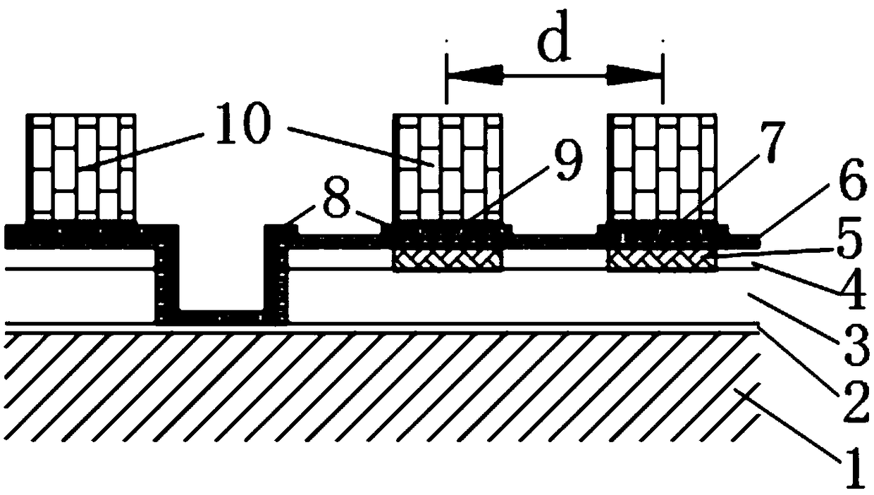
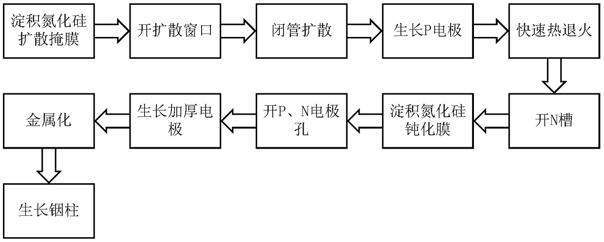
[0051] as attached figure 1 As shown, the epitaxial wafer used in this embodiment adopts metal-organic chemical vapor deposition (MOCVD) technology, and on the N-type substrate 1 with a thickness of 350 μm, an N-type InP layer 2 with a thickness of 0.5 μm is sequentially grown, and the current-carrying Subconcentration≥2×10 18 cm -3 ; InGaAs intrinsic absorption layer 3 with a thickness of 2.5 μm and a carrier concentration of 5×10 16 cm -3 ; An N-type InP cap layer 4 with a thickness of 1 μm and a carrier concentration of 5×10 16 cm -3. The large-scale small-pixel focal plane detector chip preparation process of this embodiment is based on the original process, and the order of depositing the passivation film and growing the P electrode is exchanged; the passivation film deposition process is formed by plasma enhanced chem...


PUM

PropertyMeasurementUnit
thicknessaaaaaaaaaa

Abstract

The invention discloses a method for preparing a large-scale small-pixel indium gallium arsenide focal plane detector. The method comprises the specific steps as follows: 1) depositing a silicon nitride diffusion mask, 2) opening a diffusion window, 3) performing closing-tube diffusion, 4) growing a P electrode, 5) performing rapid thermal annealing, 6) opening an N groove, 7) depositing the silicon nitride passivation film, 8) opening P and N electrode holes, 9) growing a thickened electrode, 10) metallizing, and 11) growing an indium bump. The invention has the advantages that: 1, the preparation process is simpler, and the technique of first growing the P-region electrode is used to reduce the risk of conduction between the P-region electrode and the N-region InP material caused by lithography deviation and over-etching; 2, the inductively coupled plasma chemical vapor deposition (ICPCVD) technology is used to grow the low-temperature silicon nitride passivation film, and the surface passivation layer of the chip is dense, which reduces the damage caused by the process to the surface of the material and improves the surface passivation effect; and 3, the lithographic growth technique is adopted for the metalized region and the indium bump region to reduce the contact resistance of the device.

Description

technical field [0001] The invention relates to a preparation technology of a focal plane detector, specifically a method for preparing a large-scale small pixel focal plane detector, which is suitable for preparing a high-density, high-reliability planar indium gallium arsenic focal plane detector. The above-mentioned large-scale refers to more than 2000ⅹ2000 yuan, and the above-mentioned small pixel refers to a center-to-center distance of less than 10 μm. Background technique [0002] Short-wave infrared InGaAs detectors have excellent performances such as high detection rate, high quantum efficiency, and room temperature operation, and are widely used in military, civil, and aerospace fields. With the development of short-wave infrared imaging technology to high-resolution technology, it is necessary to develop a high-performance large-scale, small pixel InGaAs focal plane detector manufacturing process. [0003] The cross-sectional structure of the InGaAs detector chip...

Claims


Application Information

Patent Timeline
Patent Type & Authority Applications(China)
IPC IPC(8): H01L31/102H01L31/18
CPCH01L31/102H01L31/184Y02P70/50
Inventor 于春蕾李雪邵秀梅龚海梅
Owner SHANGHAI INST OF TECHNICAL PHYSICS - CHINESE ACAD OF SCI
Why Eureka
Try Eureka