Heterojunction solar cell and manufacturing method thereof

A technology of solar cells and manufacturing methods, applied in circuits, photovoltaic power generation, electrical components, etc., can solve the problems of difficult control of boron diffusion process, battery grid line shielding, and high diffusion temperature, so as to avoid the reduction of minority carrier lifetime and diffusion length, The effect of avoiding damage and eliminating light loss

Active Publication Date: 2012-10-17
上海太阳能工程技术研究中心有限公司
View PDF4 Cites 4 Cited by
  • Summary
  • Abstract
  • Description
  • Claims
  • Application Information

AI Technical Summary

Problems solved by technology

However, heterojunction batteries also have a disadvantage of conventional batteries: the grid lines in front of the battery block
The existing P-N junction manufacturing method mainly

Method used


Image

  • Heterojunction solar cell and manufacturing method thereof
  • Heterojunction solar cell and manufacturing method thereof
  • Heterojunction solar cell and manufacturing method thereof

Examples


Embodiment 1

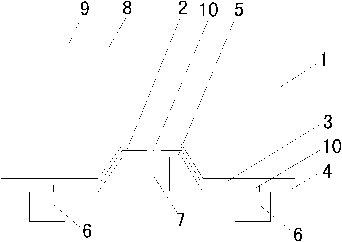
[0034] figure 1 It is a schematic cross-sectional structure diagram of a heterojunction solar cell manufactured by the manufacturing method of the present invention, figure 1 The fabrication method of the heterojunction solar cell shown includes the following steps:

[0035] (1) An N-type monocrystalline silicon wafer with a thickness of 150 μm and a resistivity of 0.3 Ωcm is used as the substrate 1 , and the surface of the substrate 1 is cleaned and textured by an alkali texturing method.

[0036] (2) On the front surface of the N-type silicon substrate 1, a layer of intrinsic amorphous silicon film is deposited by PECVD, and then a layer of N-type amorphous silicon film is deposited to form a silicon film layer 8 with a thickness of 30 nm. ;

[0037] (3) The P-type silicon thin film layer 3 and the N-type silicon thin film layer 2 are respectively deposited on the back surface of the N-type silicon substrate 1 by PECVD. Wherein the P-type silicon thin film layer 3 is a co...

Embodiment 2

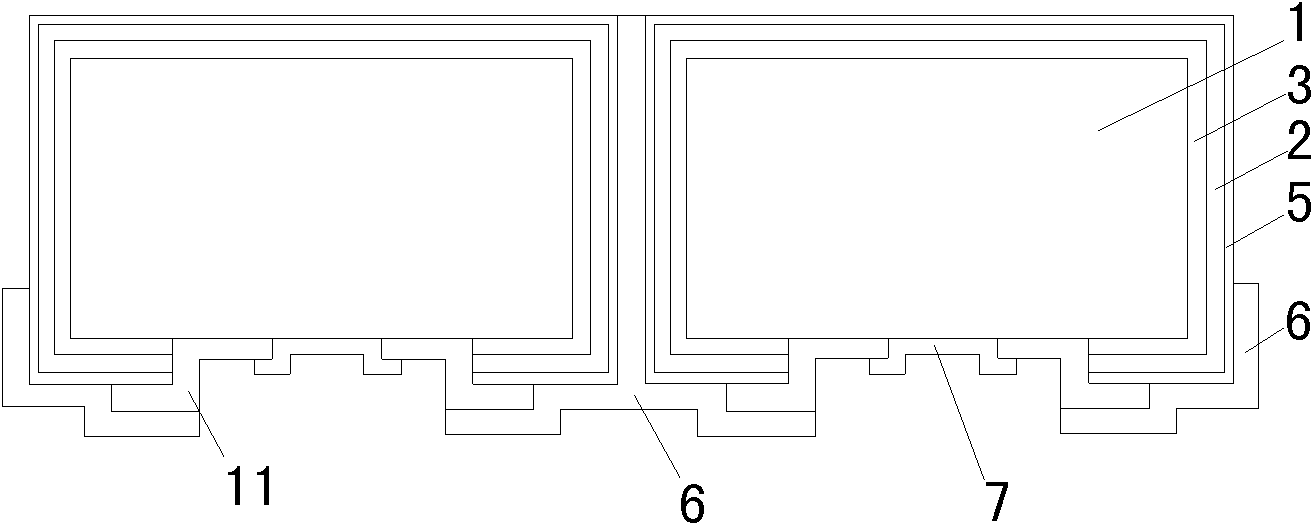
[0043] figure 2 is a schematic cross-sectional structure diagram of another heterojunction solar cell manufactured by the manufacturing method of the present invention, figure 2 The fabrication method of the heterojunction solar cell shown includes the following steps:

[0044] (1) A P-type single crystal silicon wafer with a thickness of 200 μm and a resistivity of 1 Ωcm is used as the substrate 1 , and a hole through the front and back is punched on the P-type silicon substrate 1 to form the electrode contact hole 10 .

[0045] (2) The surface of the P-type silicon substrate 1 is cleaned and textured by an alkali texturing method.

[0046] (3) The P-type silicon thin film layer 3 and the N-type silicon thin film layer 2 are respectively deposited by PECVD. Wherein the P-type silicon thin film layer 3 is a composite layer composed of the inner intrinsic amorphous silicon thin film and the outer P-type microcrystalline silicon thin film, and the N-type silicon thin film la...

Embodiment 3

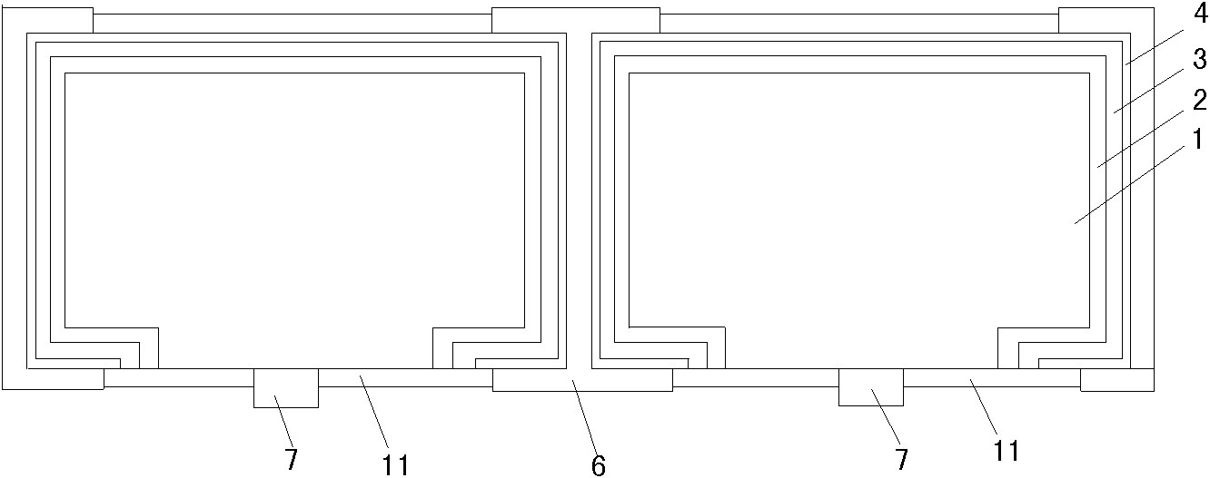
[0052] image 3 is a schematic cross-sectional structure diagram of another heterojunction solar cell manufactured by the manufacturing method of the present invention, image 3 The fabrication method of the heterojunction solar cell shown includes the following steps:

[0053] (1) A P-type monocrystalline silicon wafer with a thickness of 200 μm and a resistivity of 1 Ωcm is used as the substrate 1 , and a hole through the front and back is punched on the P-type silicon substrate 1 to form an electrode contact hole.

[0054] (2) The surface of the P-type silicon substrate 1 is cleaned and textured by an alkali texturing method.

[0055] (3) The N-type silicon thin film layer 2 and the P-type silicon thin film layer 3 are respectively deposited by PECVD. Wherein the N-type silicon film layer 2 is a composite layer composed of the inner layer intrinsic amorphous silicon film and the outer N-type nano-silicon film, and the P-type silicon film layer 3 is composed of the inner l...


PUM

PropertyMeasurementUnit
Thicknessaaaaaaaaaa
Resistivityaaaaaaaaaa
Thicknessaaaaaaaaaa

Abstract

The invention relates to a heterojunction solar cell and a manufacturing method thereof. The heterojunction solar cell comprises a crystal silicon substrate. An N-type silicon thin layer and a P-type silicon thin layer are deposited on the substrate respectively. Transparent conducting films are deposited on the N-type silicon thin layer and/or P-type silicon thin layer. Back contact structure electrodes are arranged on the transparent conducting films or/and a substrate body. The manufacturing method comprises the following steps: depositing the N-type silicon thin layer and the P-type silicon thin layer on a substrate surface; depositing the transparent conducting films on the N-type silicon thin layer and/or P-type silicon thin layer; making the electrodes; sintering so as to generate a product and so on. According to the invention, excellent surface passivation performance of a back contact cell and a low temperature technology advantage of the heterojunction cell are effectively combined; reduction of minority-carrier lifetime of a silicon material and a diffusion length is effectively avoided; a short wave response of the cell to ultraviolet light is increased and loss of a substrate resistance is decreased; light loss caused by a surface grid line is effectively reduced or eliminated.

Description

technical field [0001] The invention relates to a solar cell and a manufacturing method thereof, in particular to a heterojunction solar cell integrating the advantages of a back contact and a heterojunction cell and a manufacturing method thereof. Background technique [0002] Heterojunction solar cells can be formed by depositing an extremely thin amorphous film on crystalline silicon. The entire process is carried out below 200°C, avoiding damage to silicon wafers caused by high temperatures and increased costs caused by complex operations. Heterojunction solar cells take advantage of the wide bandgap and high photoconductivity of hydrogenated amorphous silicon and the good stability of crystalline silicon to avoid the light-induced degradation of solar cell performance (Staebler-Wronski effect) caused by the instability of amorphous silicon. In addition, the attenuation of the performance of heterojunction solar cells with the increase of temperature is also weaker than ...

Claims


Application Information

Patent Timeline
IPC IPC(8): H01L31/072H01L31/0747H01L31/0224H01L31/18H01L31/20
CPCY02E10/50Y02P70/50
Inventor 李红波张滢清张愿成庞宏杰刘穆清王凌云
Owner 上海太阳能工程技术研究中心有限公司
Why Eureka
Try Eureka