Back full-passivation contact solar cell and preparation method thereof
A solar cell and backside technology, applied in the field of solar cells, can solve problems such as incompatibility with production lines, and achieve the effects of improving production line yield, simplifying process steps, and enhancing tunnel effect.
- Summary
- Abstract
- Description
- Claims
- Application Information
AI Technical Summary
Problems solved by technology
Method used
Image
Examples
Embodiment 1
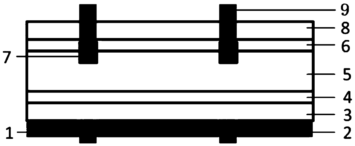
[0034] Such as figure 1 As shown, the back fully passivated contact solar cell, including back electrode 1, all aluminum back electric field 2, nanocrystalline boron hydride doped silicon carbide layer 3, silicon oxide layer 4, P-type silicon 5, n+ emitter layer 6, heavy Doped n++ emitter 7, silicon nitride anti-reflection passivation film 8 and front electrode 9, in which all-aluminum back electric field 2, nanocrystalline boron hydride doped silicon carbide layer 3, silicon oxide layer 4, P-type silicon 5, n+ The emitter layer 6 and the silicon nitride anti-reflection passivation film 8 are connected sequentially from bottom to top; one end of the heavily doped n++ emitter 7 is connected to the front electrode 9, and the other end passes through the n+ emitter layer 6 and is embedded in the P-type silicon 5 in.
[0035] In this embodiment, the back electrode 1 and the front electrode 9 are Ag electrodes.
[0036] In this embodiment, the heavily doped n++ emitter 7 is prepa...
PUM
| Property | Measurement | Unit |
|---|---|---|
| thickness | aaaaa | aaaaa |
Abstract
Description
Claims
Application Information


