Gate drive circuit

a technology of gate drive and gate gate, which is applied in the direction of pulse technique, voltage/current interference elimination, and increase in the modification of reliability, etc., and can solve problems such as difficult matter

Inactive Publication Date: 2008-10-09
SANKEN ELECTRIC CO LTD
View PDF6 Cites 14 Cited by
  • Summary
  • Abstract
  • Description
  • Claims
  • Application Information

AI Technical Summary

Benefits of technology

[0013]According to the present invention, it is possible to provide a gate drive circuit which includes monitor circuits of a simple structure and does not cause chattering in monitoring signals even at rapid turning on and off of the switching elements.

Problems solved by technology

However, such a matter is difficult.

Method used


Image

  • Gate drive circuit
  • Gate drive circuit
  • Gate drive circuit

Examples


first embodiment

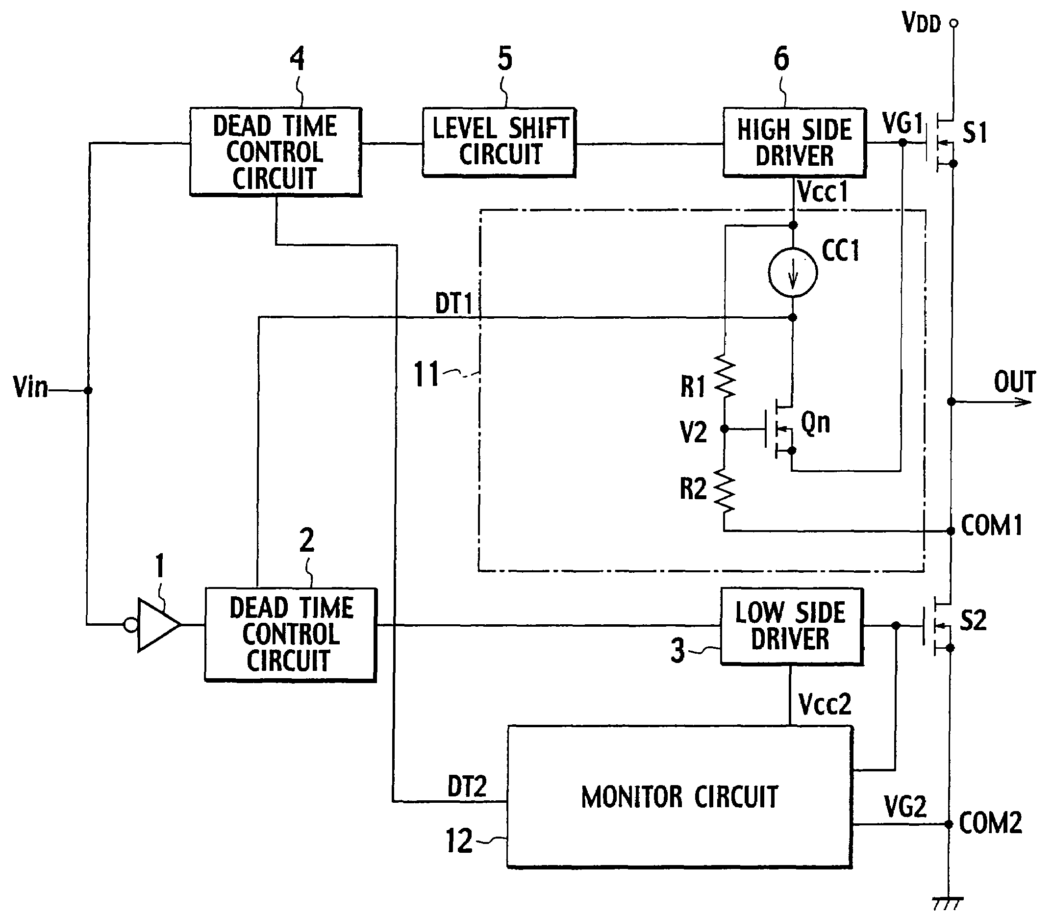
[0037]FIG. 5 is a diagram illustrating a first example of a gate drive circuit according to a first embodiment of the present invention. The gate drive circuit illustrated in FIG. 5 is characterized by including monitor circuits 11 and 12 instead of the monitor circuits 7 and 8 of the gate drive circuit as illustrated in FIG. 3. The other constitution illustrated in FIG. 5 is the same as that illustrated in FIG. 3. The same components are given the same reference numerals, and the description thereof is omitted.

[0038]The monitor circuit 11 includes a current source CC1, resistors R1 and R2, and an N-type MOSFET (N-type FET) Qn as a detector detecting an OFF state of a switching element S1. The current source CC1 may be a resistor or a current mirror circuit. Using the current source CC1 which is a constant current source allows more accurate detection of the on / off states of the switching elements S1 and S2.

[0039]An end of the current source CC1 is connected to power supply voltage ...

second embodiment

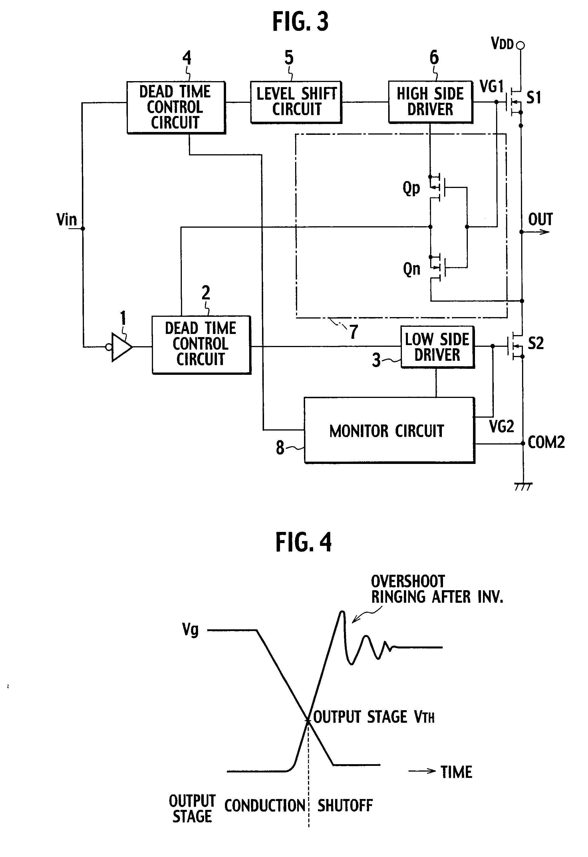
[0047]FIG. 10 is a diagram illustrating a gate drive circuit according to a second embodiment of the present invention. The second embodiment illustrated in FIG. 10 is characterized by further including a P-type FET Qp as a shutoff means constituting a power saving circuit in the monitor circuit of the first embodiment illustrated in FIG. 5.

[0048]The source of the P-type FET Qp is connected to the power supply voltage Vcc1; the drain of the P-type FET Qp is connected to an end of the resistor R1; and the gate of the P-type FET Qp is connected to an input voltage DIN1 of the high side driver 6. When the voltage DIN1 is turned off (when a signal is inputted from the other monitor circuit 12), the P-type FET Qp is turned on, and the voltage V2, which is obtained by dividing the power supply voltage Vcc1 by the resistors R1 and R2, is applied to the gate of the N-type FET Qn to turn on the N-type FET Qn.

[0049]When the voltage DIN1 is high (when a signal from the other monitor circuit 12...

third embodiment

[0050]FIG. 11 is a diagram illustrating a gate drive circuit according to a third embodiment of the present invention. The third embodiment illustrated in FIG. 11 is characterized by further including a Zener-diode ZD1 as a stabilization circuit in the monitor circuit of the second embodiment illustrated in FIG. 10. The cathode of the Zener-diode ZD1 is connected to the connection point of the drain of the P-type FET Qp and the resistor R1, and the anode thereof is connected to an end of the resistor R2.

[0051]The drain voltage of the P-type FET Qp is therefore clamped to breakdown voltage of the Zener diode ZD1, thus suppressing variations of the power supply voltage Vcc1 or variations of the divided voltage V2 due to variations of on resistance of the P-type FET Qp. This makes it possible to stably monitor the on / off states of the switching elements S1 and S2.


PUM


Abstract

A gate drive circuit including dead time control circuits delaying on periods of switching elements S1, S2 based on a control signal; driving circuits; and monitor circuits. Each of the monitor circuits includes a current source and an N-type FET in which the source is connected to the gate of one of the switching elements; the drain is connected to the current source; and a predetermined voltage is applied to the gate. When an off state of one of the switching elements is detected, the N-type FET Qn outputs an off signal to the dead time control circuit on the other switching element side. Based on the off signal, the dead time control circuit on the other switching element side terminates an operation of delaying the on period of the other switching element.

Description

BACKGROUND OF THE INVENTION[0001]The present invention relates to a gate drive circuit to prevent two switching elements connected in series from simultaneously conducting electricity.[0002]FIG. 1 is a diagram illustrating a first example of a related gate drive circuit. FIG. 2 is an operation waveform diagram of the first example of the related gate drive circuit. In FIG. 1, a series circuit of a switching element S1 composed of a MOSFET and a switching element S2 composed of a MOSFET is connected to between a DC power supply voltage VDD and the ground. This gate drive circuit turns on and off alternately the switching elements S1 and S2 based on a control signal Vin and intermittently outputs the DC power supply voltage VDD to a terminal OUT. The gate drive circuit includes an inverter 1, dead time control circuits 2 and 4, a low side driver 3, a level shift circuit 5, and a high side driver 6.[0003]The inverter 1 inverts the control signal Vin and outputs the same to the dead tim...

Claims


Application Information

Patent Timeline
Patent Type & Authority Applications(United States)
IPC IPC(8): H03L7/00
CPCH03K5/1515H03K17/165H03K17/6871H03K19/00361
Inventor SUZUKI, MIOTAKAHASHI, HIROSHIUENO, MASAO
Owner SANKEN ELECTRIC CO LTD
Why Eureka
Try Eureka