Media case and circuit pattern sheet

Inactive Publication Date: 2008-10-09
HITACHI LTD
View PDF8 Cites 44 Cited by
  • Summary
  • Abstract
  • Description
  • Claims
  • Application Information

AI Technical Summary

Benefits of technology

[0008]The present invention can provide a media case and a circuit pattern sheet in a sim

Problems solved by technology

Therefore, it has been difficult to increase stack density of the housing cases for saving space.
In addition, the read antenna has to previously be connected to the read writer apparatus, which gives rise to a problem that wiring becomes complicated and the configuration is made inflexible.
Moreover, any of the booster coil and the on-chip coil on the chip is complicated in its structure and manufacturi

Method used


Image

  • Media case and circuit pattern sheet
  • Media case and circuit pattern sheet
  • Media case and circuit pattern sheet

Examples


first embodiment

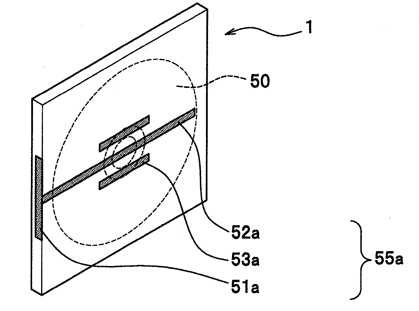
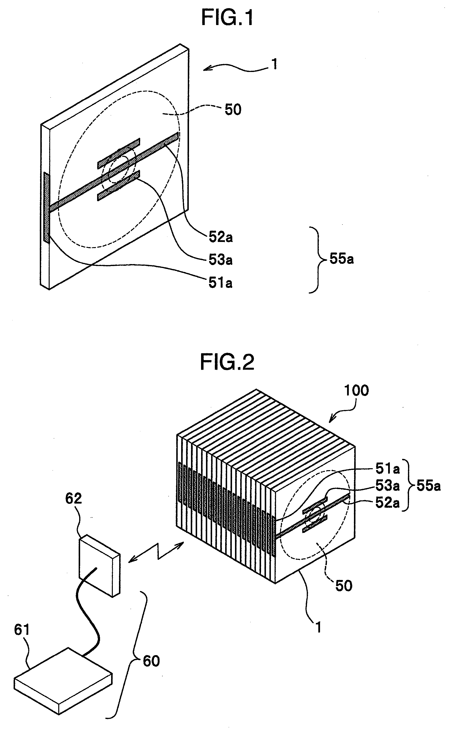
[0029]FIG. 1 is a perspective view illustrating a media case 1 of a first embodiment according to the present invention. Here, in the case where the base member of the media case 1 is transparent will be illustrated. This base member can be dyed or be opaque.

[0030]This media case 1 is a container which houses disk media 50 in the inner space and is freely opened and closed and made of dielectric such as rigid plastic including styrene resin, acrylic resin and polycarbonate and paper. In the media case 1, a circuit pattern 55a made of high-frequency good conductor film such as aluminum and copper is formed. That is, the circuit pattern 55a made of electrically conductive film is formed on the base member of the disk media 50 made of dielectric and thereby a stripline waveguide is configured. The circuit pattern 55a has thickness capable of providing sufficient low resistance for high frequency signals and formed by etching and sputtering, for example, or by attaching metal foil. In a...

second embodiment

[0054]FIG. 5 is a perspective view illustrating a media case 2 of a second embodiment according to the present invention.

[0055]This media case 2 includes the antenna element 51a being formed in the position adjacent to the back plane in the flat plate portion to become the lid part or the plate part instead of forming the back face of the media case 1 (see FIG. 1). The other configurations can be likewise the media case 1 (see FIG. 1) of the first embodiment.

[0056]According to the second embodiment of the media case 2, the antenna element 51a is adjacent to the back plane and, therefore, the effect approximately likewise the effect of the media case 1 of the first embodiment is obtained. In addition, the antenna element 51a, the waveguide line 52a and the resonance element 53a can be formed on the same flat plane and, therefore, can be formed more easily. Moreover, no designs, letters and the like printed on the back plane label (the bent part corresponds to the back plane of the re...

third embodiment

[0057]FIG. 6 is a perspective plan view illustrating a media case 3 of a third embodiment according to the present invention.

[0058]In this media case 3, two antenna elements 51b configuring a dipole antenna being on its back plane or formed on its back plane with its ends being arranged in a small distance; two waveguide lines 52b extending in parallel along the direction of diameter of the disk media 50 from the two adjacent parts of the antenna element 51b to become a feed part of this dipole antenna and the four (two pairs of) resonance elements 53b formed in the vicinity of the center of the disk media 50 in parallel in a determined distance to those two waveguide lines 52b are formed.

[0059]The length L1 of the antenna element 51b is, for example, L1=(1 / 2)λ, where the wavelength λ of electromagnetic waves of frequencies to be exchanged. In addition, the length L2 of the resonance element 53a is, for example, L2=(1 / 2)λ. The length of the waveguide line 52b is at least such length...


PUM


Abstract

A media case and a circuit pattern sheet with a simple configuration is provided that allows highly dense collection and reliable recognition of housed disk media.
The media case 1 can house disk media 50 provided with an RFID tag (not illustrated in the drawing). This media case 1 includes an antenna element 51a being formed on its back plane to exchange an electromagnetic wave signal with the outside of the media case 1; a waveguide line 52a formed in the vicinity of its center therethrough along the disk media 50 from the antenna element 51a to guide high-frequency signals representing the electromagnetic wave signals to the antenna element 51a; and a resonance element 53a being formed adjacent to this waveguide line 52a and electromagnetically induced by the high-frequency signal.

Description

INCORPORATION BY REFERENCE[0001]The present application claims priority from Japanese application JP2007-097223 filed on Apr. 3, 2007, the content of which is hereby incorporated by reference into this application.BACKGROUND OF THE INVENTION[0002]The present invention relates to a media case, and a circuit pattern sheet, which can house disk media provided with an RFID (Radio Frequency Identification) tag allowing information recorded on an IC chip to be read in a noncontact manner outside it.[0003]It is conceivable to apply a noncontact tag to disk media with its content being written in the tag in order to manage the disk media. Most portions of such disk media including its outer periphery are used for a data storage region having a data storage layer. However, no data storage layer is present in the vicinity of a hole in the center in order to clamp the disk media in use. From this point of view, a noncontact tag is preferably located in the vicinity of a hole in the center of t...

Claims


Application Information

Patent Timeline
IPC IPC(8): G08B13/14
CPCG11B33/0411H01Q1/22H01Q1/2208H01Q1/38B65D85/544B65G1/137G06K19/07G11B23/30
Inventor SAKAMA, ISAOHOSHINO, OSAMU
Owner HITACHI LTD
Why Eureka
Try Eureka