

Defect inspecting apparatus and defect-inspecting method
- Summary
- Abstract
- Description
- Claims
- Application Information
AI Technical Summary
Benefits of technology
Problems solved by technology
Method used
Image

Examples
Embodiment Construction
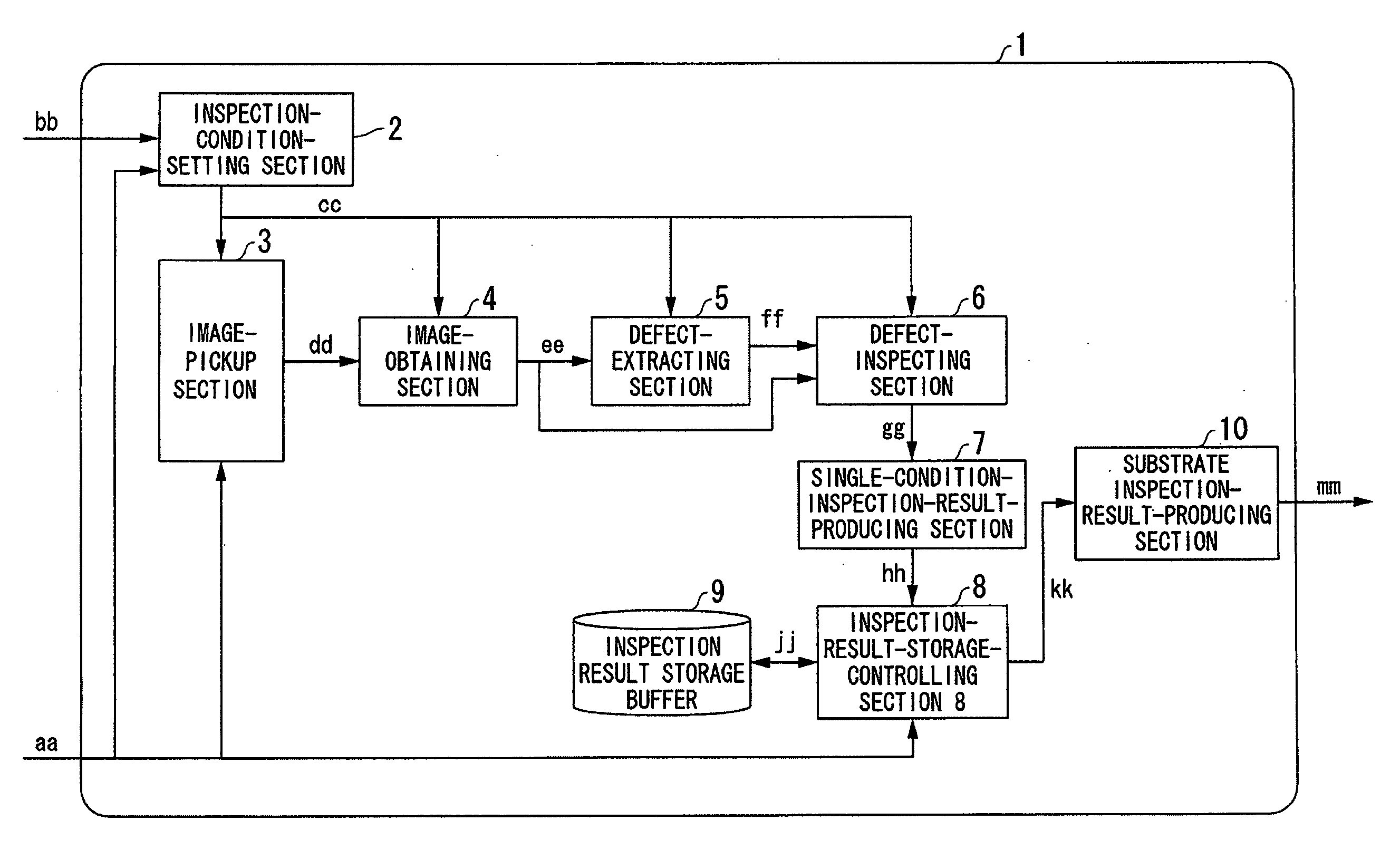
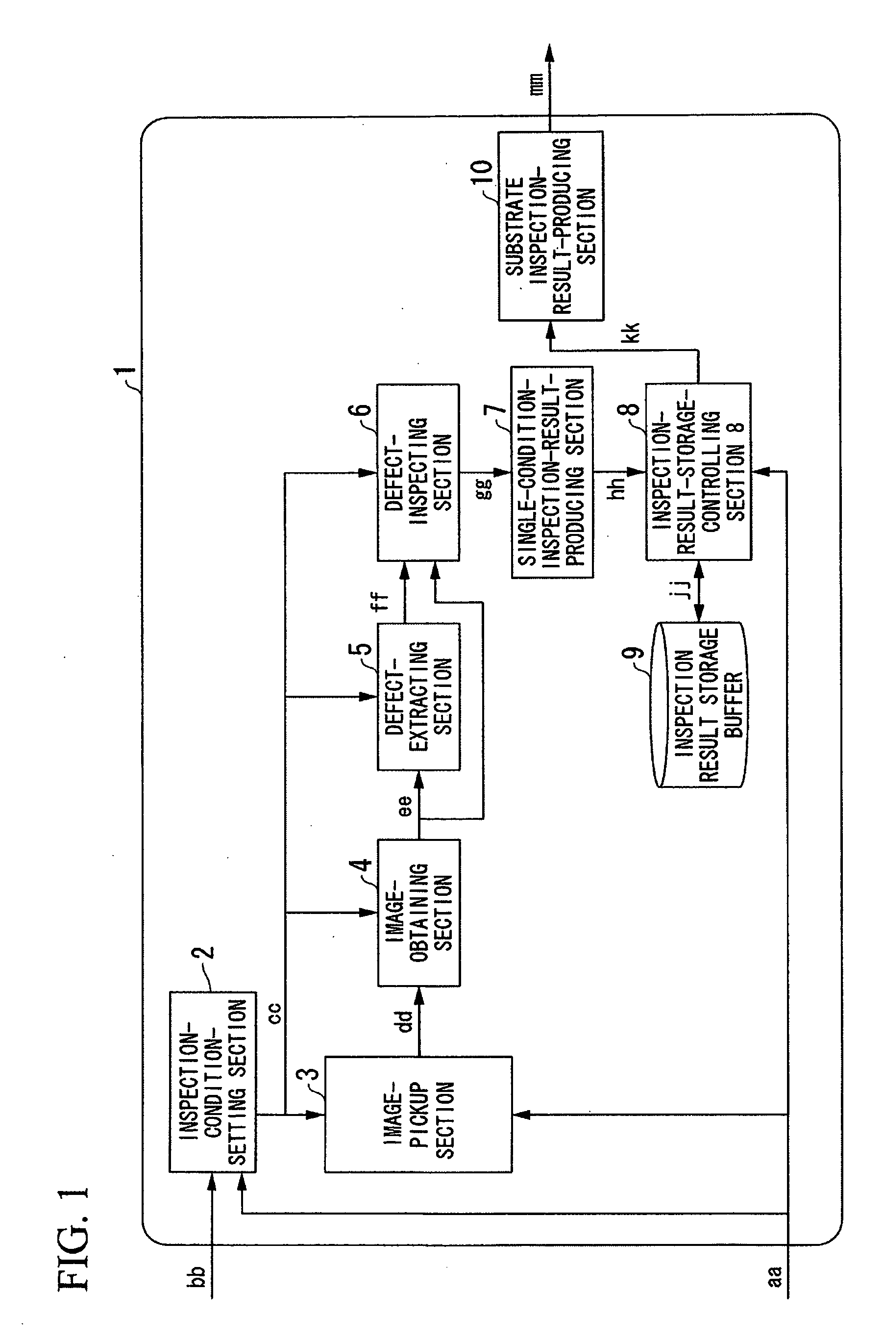
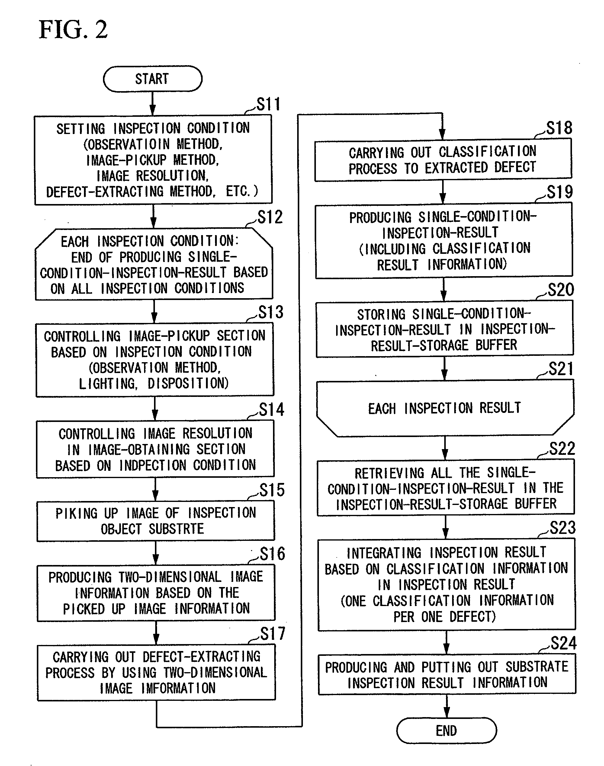
[0028]An embodiment of the present invention will be explained below with reference to the drawings. The present embodiment relates to a macro inspection apparatus for semiconductor wafer adapted to the present invention. FIG. 1 is a schematic diagram of an inspection apparatus according to the present embodiment. An inspection apparatus 1 receives externally inputted information including control information aa for controlling the apparatus; and substrate information bb indicating information associated with an inspection object substrate (inspection object) such as design information indicating the substrate type, process, and size and position of a chip and shot, etc. Furthermore, information output from the inspection apparatus 1 is inspection-result information mm associated with the inspection object substrate.
[0029]The control information aa and the substrate information bb upon being put into the inspection apparatus 1 are first received by an inspection-condition-setting se...
PUM
 Abstract
Description
Claims
Application Information