Method of manufacturing bonded wafer

a manufacturing method and semiconductor technology, applied in semiconductor/solid-state device manufacturing, basic electric elements, electric devices, etc., can solve the problems of no improvement in roughness and no siosub>2 reaction, and achieve the effect of suppressing interface roughness and low surface roughness

Active Publication Date: 2008-10-09
SUMCO CORP
View PDF10 Cites 7 Cited by
  • Summary
  • Abstract
  • Description
  • Claims
  • Application Information

AI Technical Summary

Benefits of technology

[0013]An aspect of the present invention provides for a method of manufacturing a final product in the form of a bonded substrate having low surface roughness by suppressing interface roughness between a

Problems solved by technology

However, even when an ultra-high temperature heat treatment is conducted following bonding, the SiO2 reaction has been found not to

Method used


Image

  • Method of manufacturing bonded wafer
  • Method of manufacturing bonded wafer
  • Method of manufacturing bonded wafer

Examples


example 1

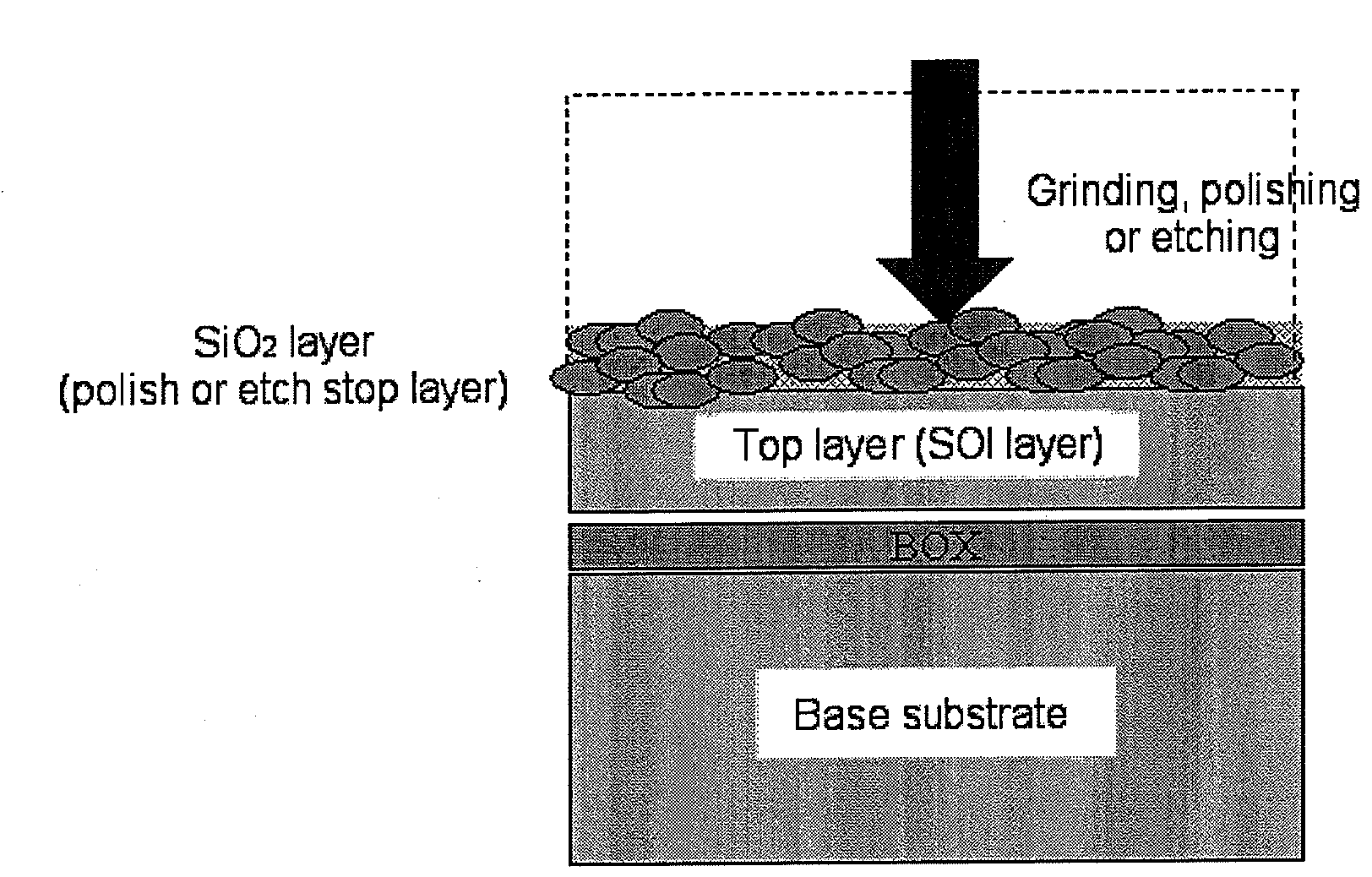
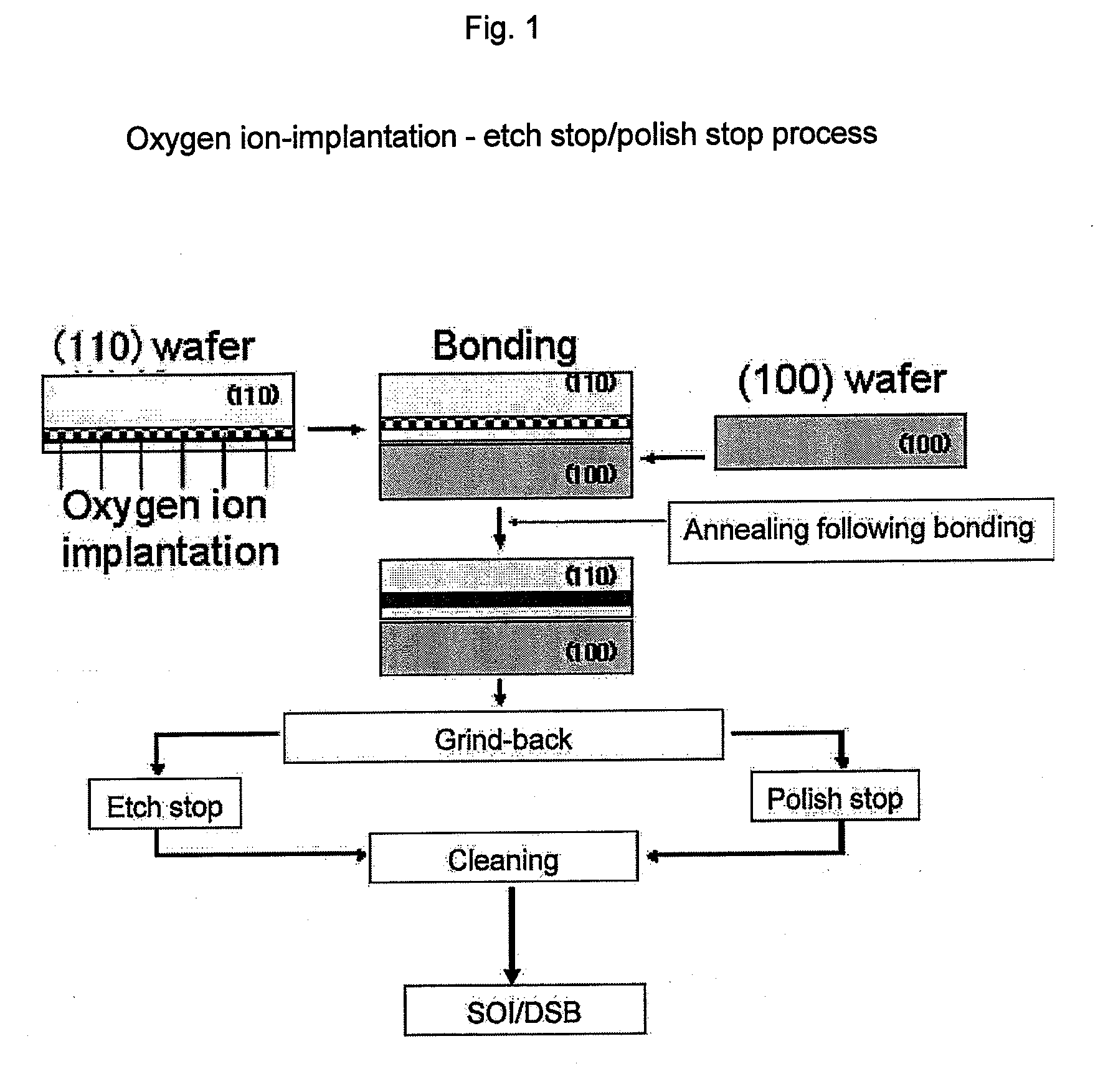
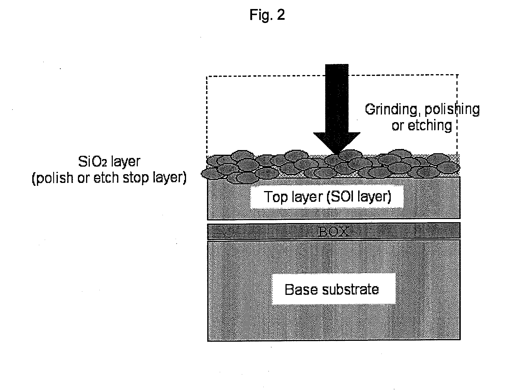
[0062]A bonded wafer with a SOI structure was fabricated by the following steps (1) to (9):[0063](1) A 300 mm base wafer was prepared. The 300 mm base wafer was a p-type wafer (100) with a substrate resistivity of 10 to 20 Ωcm and had a BOX layer (1,500 Angstroms) formed by heat treatment in an oxygen atmosphere for 5 hours at 1,000° C.[0064](2) A 300 mm active layer wafer (top substrate) was prepared. The 300 mm active layer wafer was a p-type wafer (100) with a substrate resistivity ranging from 0.001 to 10 Ωcm (as described, in detail, in Table 1) that had an oxygen ion implantation layer. The oxygen ion implantation layer was formed under conditions of an acceleration voltage of 180 keV, a dose of 2e17cm−2, and a substrate temperature of 100 to 500° C.[0065](3) The base wafer and active layer wafer were SC1 washed and bonded.[0066](4) Following bonding, a bond-strengthening heat treatment was conducted for 1 hour at 1,200° C. (in an oxygen atmosphere).[0067](5) The surface of th...

example 2

[0074]A bonded wafer with a DSB structure was fabricated by the following steps (1) to (9):[0075](1) A 300 mm base wafer was prepared. The 300 mm base wafer was a p-type wafer (100) with a substrate resistivity of 10 to 20 Ωcm.[0076](2) A 300 mm active layer wafer (top substrate) was prepared. The 300 mm active layer wafer was a p-type wafer (110) with a substrate resistivity ranging from 0.001 to 10 Ωcm (as shown in Table 1) that had an oxygen ion implantation layer. The oxygen ion implantation layer was formed under conditions of an acceleration voltage of 180 keV, a dose of 2e17cm−2, and a substrate temperature of 100 to 500° C.

Steps (3) to (9) were implemented in the same manner as in Example 1.

[0077]The evaluation results are given in Table 1.

TABLE 1Relation between resistivity and roughnessSurfaceroughnessRMSTop substrate[Angstroms]Structureresistivity [Ωcm](10 μm × 10 μm)1Comp. Ex.SOI1011.02Comp. Ex.SOI112.23Comp. Ex.SOI0.212.74Example ofSOI0.17.3present invention5Ex. ofSOI0....


PUM


Abstract

The present invention provides a method of manufacturing a bonded wafer. The method includes forming an oxygen ion implantation layer in an active layer wafer having a substrate resistivity of 1 to 100 mΩcm by implanting oxygen ions in the active layer wafer, bonding a base wafer and the active layer wafer directly or through an insulating layer to form a bonded wafer, heat treating the bonded wafer to strengthen the bond and convert the oxygen ion implantation layer into a stop layer, grinding, polishing, and/or etching, from the active layer wafer surface side, the bonded wafer in which the bond has been strengthened to expose the stop layer on a surface of the bonded wafer, removing the stop layer, and subjecting the bonded wafer from which the stop layer has been removed to a heat treatment under a reducing atmosphere to diffuse an electrically conductive component comprised in the active layer wafer.

Description

CROSS-REFERENCE TO RELATED APPLICATIONS[0001]This application claims the benefit of priority under 35 USC 119 to Japanese Patent Application No. 2007-097197, filed on Apr. 3, 2007, which is expressly incorporated herein by reference in its entirety.BACKGROUND OF THE INVENTION[0002]1. Field of the Invention[0003]The present invention relates to a method of manufacturing a semiconductor substrate. More particularly, the present invention relates to a method of manufacturing an oxygen ion-implanted—etch / polish stop bonded substrate affording improved SiO2 / Si interface roughness by using a wafer with a substrate resistivity of 1 to 100 mΩcm as a wafer on the active layer side. The manufacturing method of the present invention can be applied to both silicon-on-insulator (SOI) and direct silicon bonding (DSB) substrates.[0004]2. Discussion of the Background[0005]In contrast to conventional silicon wafers, SOI wafers provide superior features, such as device isolation, reduced parasitic ca...

Claims


Application Information

Patent Timeline
IPC IPC(8): H01L21/30
CPCH01L21/76243H01L21/76251H01L21/20
Inventor ENDO, AKIHIKOMORIMOTO, NOBUYUKI
Owner SUMCO CORP
Why Eureka
Try Eureka