Method for aligning microscopic structures and substrate having microscopic structures aligned, as well as integrated circuit apparatus and display element

a technology of microscopic structures and integrated circuits, applied in electrostatic separators, diaphragms, electrolysis, etc., can solve the problems of insufficient control of aligning nanostructures, achieve high yield, improve the alignment of silicon nanowires, and increase the freedom in terms of the manner in which voltage can be applied significantly.

Inactive Publication Date: 2008-10-16
SHARP KK +1
View PDF4 Cites 46 Cited by
  • Summary
  • Abstract
  • Description
  • Claims
  • Application Information

AI Technical Summary

Benefits of technology

[0010]The above-described configuration makes it possible to align microscopic structures in desired locations and in a desired direction with accurate control, and thus, makes so-called high-precision alignment possible. Accordingly, when microscopic structures aligned with high precision according to the present invention are used as devices, it becomes possible to make an integrated circuit, a display, and the like, high-performance, as well as to manufacture them with high yield.
[0011]Furthermore, the freedom in terms of a manner in which voltages can be applied significantly increases because there are three electrodes, and therefore, it becomes possible to improve alignment of silicon nanowires a great deal.
[0012]The method for aligning microscopic structures according to the first embodiment of the present invention makes it possible to align microscopic structures in desired locations and in a desired direction with accurate control and high precision. Accordingly, it becomes possible to make an integrated circuit, a display, and the like high-performance using microscopic structures as devices, as well as to manufacture them with high yield.
[0013]Furthermore, the freedom in terms of the manner in which voltages can be applied significantly increases because there are three electrodes, and therefore, it becomes possible to improve alignment of silicon nanowires a great deal.

Problems solved by technology

According to conventional methods, however, there isn't sufficiently accurate control in aligning nanostructures.

Method used


Image

  • Method for aligning microscopic structures and substrate having microscopic structures aligned, as well as integrated circuit apparatus and display element
  • Method for aligning microscopic structures and substrate having microscopic structures aligned, as well as integrated circuit apparatus and display element
  • Method for aligning microscopic structures and substrate having microscopic structures aligned, as well as integrated circuit apparatus and display element

Examples


first embodiment

[0120]A first embodiment of the present invention is described in reference to FIGS. 11 to 18. FIG. 11 shows an insulating substrate used in the first embodiment. FIG. 12 is a diagram illustrating the principle of the alignment of microscopic structures. FIG. 13 is a diagram showing a first example of preferable potentials to be applied to electrodes when the microscopic structures are aligned. FIG. 14 is a diagram showing a second example of preferable potentials to be applied to the electrodes when the microscopic structures are aligned. FIG. 15 is a diagram illustrating the state of alignment of the microscopic structures at the time when the microscopic structures are aligned. FIG. 16 is a diagram illustrating the principle of the effects gained at the time when the microscopic structures are aligned. FIG. 17 is a diagram showing a third example of preferable potentials to be applied to the electrodes when the microscopic structures are aligned. FIG. 18 is a diagram showing a fo...

second embodiment

[0159]A second embodiment of the present invention is described in reference to FIGS. 19 to 25. FIG. 19 shows an insulating substrate used in the present embodiment. FIGS. 20 to 23 are diagrams illustrating the procedure of the method for aligning microscopic structures according to the present embodiment. FIG. 24 is a diagram showing the state during the process for aligning microscopic structures in the present embodiment. FIG. 25 is a diagram illustrating preferable potentials to be applied to the electrodes in the state in FIG. 24.

[0160]The method for aligning microscopic structures according to the second embodiment of the present invention includes a substrate preparing step of preparing an insulating substrate where one or more microscopic structure-aligning regions having as an unit fourth, fifth and sixth electrodes to which independent potentials are applied are formed; a microscopic structure applying step of applying a liquid including microscopic structures ranging from...

third embodiment

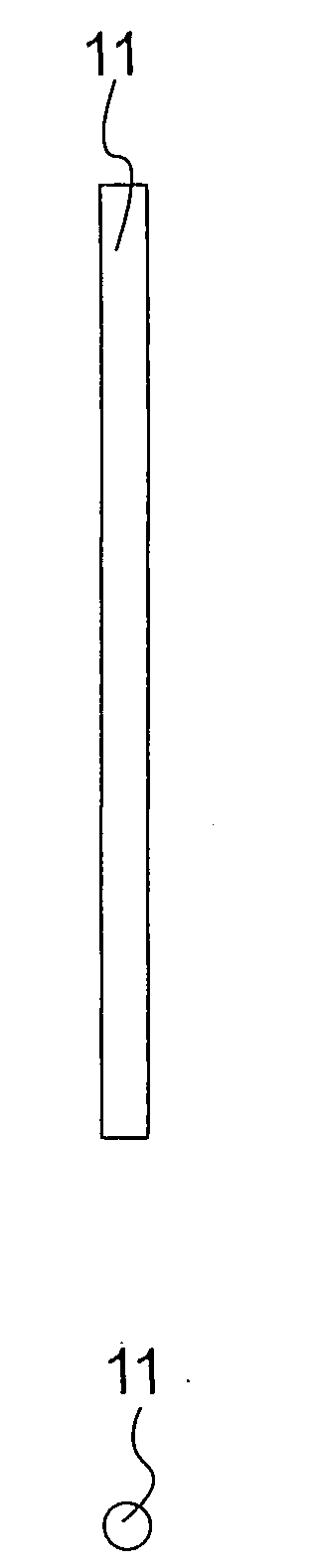
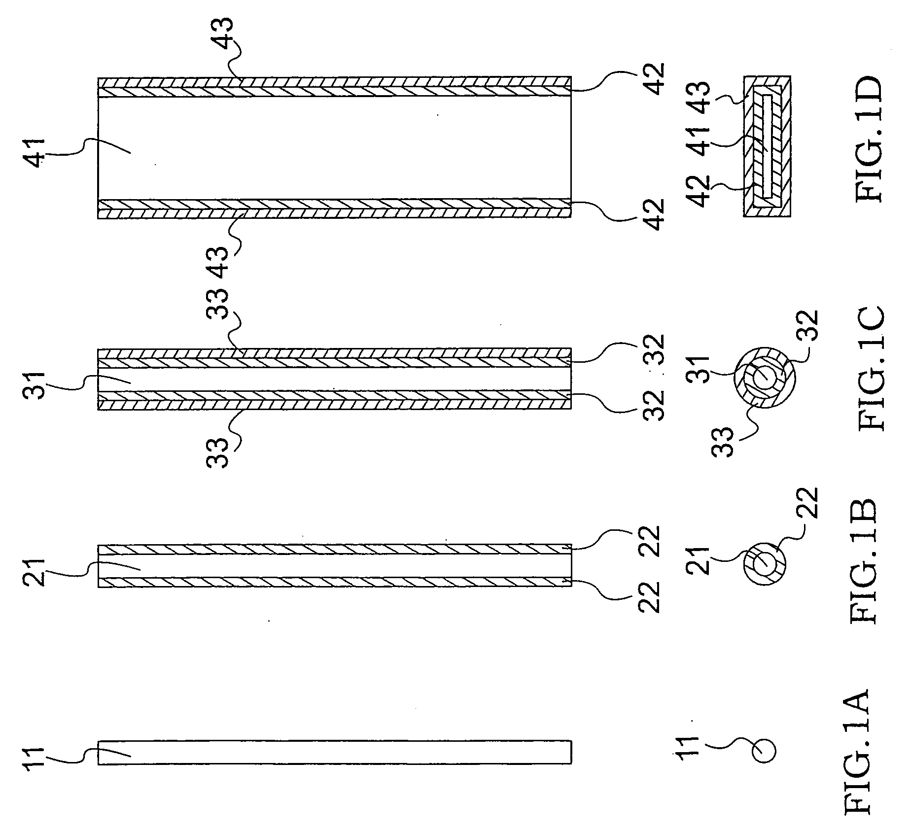
[0172]The third embodiment of the present invention is an example of a device and an integrated circuit using the microscopic structures aligned in the first and second embodiments. A case as that above, where microscopic structures having the configuration in FIG. 1B are applied as devices, is described in the present embodiment.

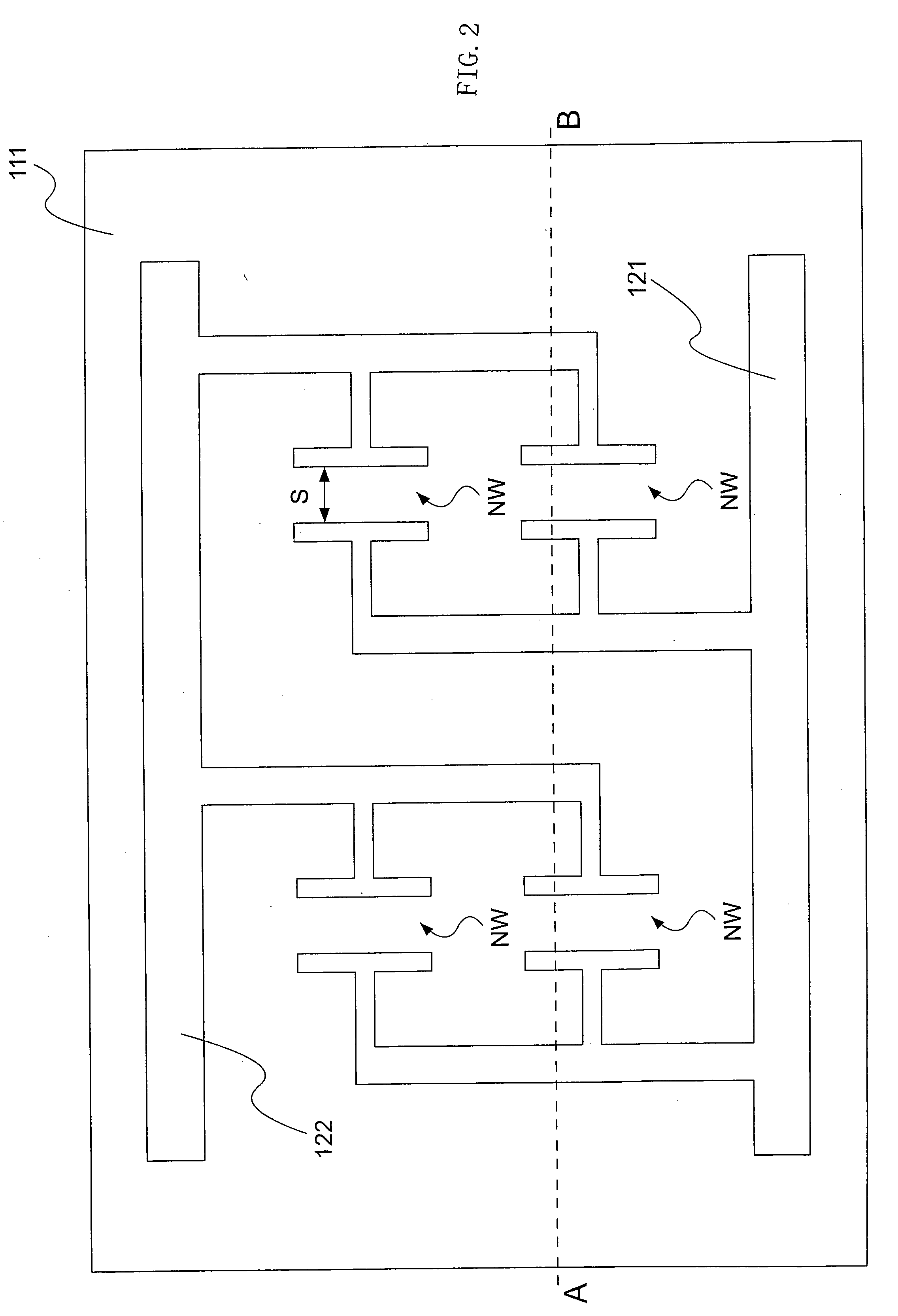
[0173]The present embodiment is described in reference to FIGS. 26 and 27. A case where two nanowire elements (N channel type and P channel type) are placed on the same substrate is described in the present embodiment as a concrete example of an integrated circuit apparatus. The integrated circuit apparatus according to the present invention may, of course, have a configuration where three or more elements having different functions are provided on the same substrate.

[0174]FIG. 26 is a plan diagram showing wires on a substrate where an integrated circuit apparatus 1 is formed as a portion of the integrated circuit apparatus according to the present inventio...


PUM

PropertyMeasurementUnit
Timeaaaaaaaaaa
Angleaaaaaaaaaa
Timeaaaaaaaaaa

Abstract

An object of the present invention is to implement a method for aligning microscopic structures in desired locations and in a desired direction, in order to align microscopic structures, such as nanostructures, with high precision. The method includes a substrate forming step of forming three electrodes to which independent potentials can be applied, a microscopic structure liquid applying step of applying a liquid in which microscopic structures are dispersed to the insulating substrate, and a microscopic structure aligning step of applying respective voltages to the three electrodes to align the microscopic structures in locations defined by the electrodes.

Description

CROSS-REFERENCE TO RELATED APPLICATION[0001]This application is related to Japanese Patent Application No. 2007-102848 filed on Apr. 10, 2007, whose priority is claimed under 35 USC § 119, the disclosure of which is incorporated by reference in its entirety.BACKGROUND OF THE INVENTION[0002]1. Field of the Invention[0003]The present invention relates to a method for aligning microscopic structures and a substrate having microscopic structures aligned, as well as an integrated circuit apparatus and a display element. In particular, the present invention relates to a method for aligning microscopic structures in desired locations and a substrate having microscopic structures aligned in desired locations, as well as an integrated circuit apparatus and a display having devices formed of microscopic structures aligned in desired locations in accordance with the method for aligning microscopic structures.[0004]2. Description of the Related Art[0005]In recent years, use of nanostructures, s...

Claims


Application Information

Patent Timeline
IPC IPC(8): C25D1/12
CPCC25D13/02C25D13/18H01L21/76838H01L23/544H01L29/0665H01L29/0673H01L2924/0002H01L29/78696H01L2221/1094H01L2924/19043H01L2924/00
Inventor SHIBATA, AKIHIDEOKADA, YASUNOBU
Owner SHARP KK
Why Eureka
Try Eureka