High Current Steering ESD Protection Zener Diode And Method

a technology of zener diodes and high current, applied in the field of n +/p + zener diodes, can solve the problems of not providing a low resistance path to ground, zener devices are susceptible to damage from electrostatic discharge, and it takes longer for zener devices b>220/b> to completely turn, etc., to achieve the effect of increasing the current handling capability and improving the speed of operation

Inactive Publication Date: 2008-10-23
SEMICON COMPONENTS IND LLC
View PDF11 Cites 14 Cited by
  • Summary
  • Abstract
  • Description
  • Claims
  • Application Information

AI Technical Summary

Benefits of technology

[0007]The present invention relates to an N+ / P+ zener diode where the implanted regions are designed to steer the current flow away from the sidewalls of the diode and towards the bottom walls in order to induce uniform reverse breakdown, thereby leading to improved speed of operation and increase in current handling capability.

Problems solved by technology

MOS devices are susceptible to damage from electrostatic discharge, or ESD.
As such, with this breakdown profile, it takes longer for the zener device 220 to completely turn on, and does not provide a low resistance path to ground.

Method used


Image

  • High Current Steering ESD Protection Zener Diode And Method
  • High Current Steering ESD Protection Zener Diode And Method
  • High Current Steering ESD Protection Zener Diode And Method

Examples


Embodiment Construction

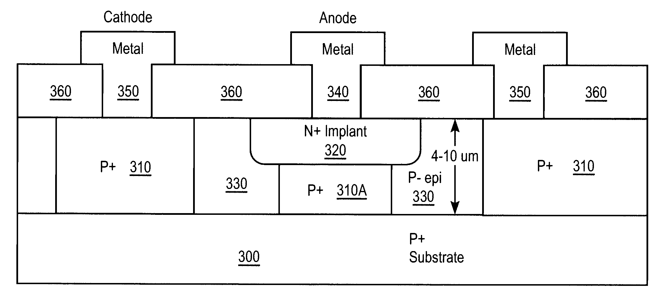
[0015]Referring first to FIG. 3, a first implementation of the invention is illustrated. The substrate 300 is formed of P+ doped material. Although this first implementation is described with respect to a P+ substrate, and layers corresponding thereto above this P+ substrate 300, it will be understood that the present invention can be implemented with an N+ substrate, and corresponding layers above, as is known in the art. A P− epitaxial layer 330 is grown over the P+ substrate. Within the epitaxial layer, a P+ sinker region 310 is created. Over a central region 310A of the sinker layer there is an N+ implant region 320. Surrounding the N+ implant 320, and extending below a bottom surface 322 of the N+ implant 320, is the P− epitaxial region 330 As shown, the portion of the P− epitaxial region adjacent to the N+ implant region has a width of X+Y, where the values of X and Y are determined based on the implant conditions, total thermal out diffusion, and photolithographic mask bias. ...


PUM


Abstract

A method of fabricating a N+/P+ zener diode where the reverse breakdown occurs in a controlled, and uniform manner leading to improved speed of operation and increase in current handling capability.

Description

FIELD OF THE INVENTION [0001]The present invention relates to an N+ / P+ zener diode where the implanted regions are designed to steer the current flow away from the sidewalls of the diode and more toward the bottom walls in order to induce uniform reverse breakdown leading to improved speed of operation and increase in current handling capability.BACKGROUND OF THE INVENTION[0002]MOS devices are susceptible to damage from electrostatic discharge, or ESD. While numerous techniques have been developed to protect MOS devices, there has been a need for an ESD-protection device and method which could be fabricated through simple semiconductor manufacturing techniques.[0003]One such known ESD-protection device is illustrated in FIGS. 1 and 2. As shown in FIG. 1, a conventional P type substrate 100 is provided, with an epitaxial layer 110 of P-material formed thereon in a conventional manner. Using CMOS fabrication techniques, a P type implant 120 is formed into and through the epitaxial lay...

Claims


Application Information

Patent Timeline
Patent Type & Authority Applications(United States)
IPC IPC(8): H01L29/866G05F1/00H01L21/20
CPCH01L27/0255H01L29/66106H01L29/866
Inventor GEE, HARRY YUEWHITWORTH, ADAM J.SHARMA, UMESH
Owner SEMICON COMPONENTS IND LLC
Why Eureka
Try Eureka