Semiconductor device stack package, electronic apparatus including the same, and method of manufacturing the same

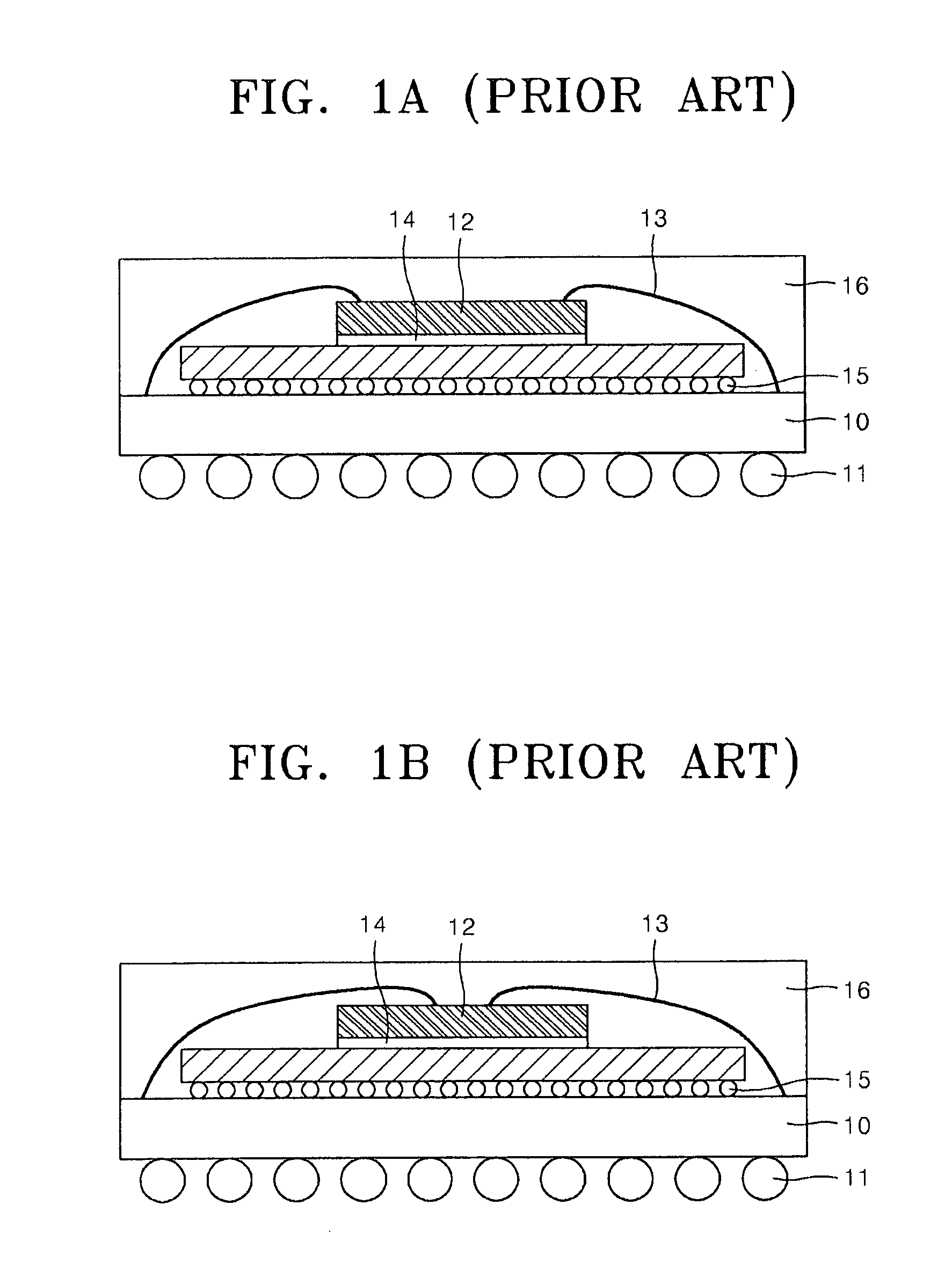
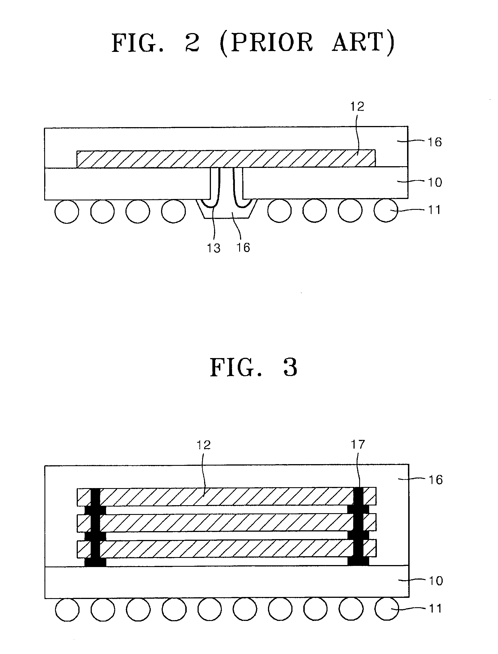
a technology of semiconductor devices and stack packages, which is applied in the direction of semiconductor devices, semiconductor/solid-state device details, electrical equipment, etc., can solve the problems of hindering the height reduction of the stack package, electrical short circuits, and difficulty in connecting the upper chips of the stack structure formed of two or more layers, so as to reduce the length of the electrical path, improve the electrical performance of the package, and not increase the height of the semiconductor device stack package

Inactive Publication Date: 2008-10-23
SAMSUNG ELECTRONICS CO LTD
View PDF10 Cites 12 Cited by
  • Summary
  • Abstract
  • Description
  • Claims
  • Application Information

AI Technical Summary

Benefits of technology

[0038]In the semiconductor device stack package according to the embodiments of the present invention, since no wire loops are included, the height of the semiconductor device stack package is not increased, and the electrical performance of the package is improved by reducing the length of the electrical path. Also, the stack package is formed of a flip chip configuration and a plurality of chips can be stacked, and the stack package can be used in various manners. Also, a heat spreader can be attached to the semiconductor device stack package to efficiently radiate heat.
[0039]The electric performance of the semiconductor device stack package is improved by reducing the length of the electrical path, and as no wire bonding is used, wire sweeping which is possibly generated during encapsulation is prevented and the stack height of the semiconductor device stack package can be reduced. The stack package according to the embodiments of the present invention further includes a heat spreader on a back side of an uppermost chip, thereby efficiently dissipating heat generated within the semiconductor device stack package.

Problems solved by technology

However, in the flip chip method, it is difficult to connect the upper chips of a stack structure formed of two or more layers.
Long wires can be the source of electrical short circuits as a result of the wire sweeping phenomenon that can occur during a molding process for thermal protection and can hinder height reduction of the stack package.
That is, although the wire bonding and flip chip methods are combined in a single package, the package still suffers from the limitation of the wire length of wire loops being too long, and thus the electrical performance and manufacturing reliability of the package can be hindered, and, at the same time, it can be difficult to reduce the overall package height.
In detail, since the upper semiconductor device is of a wire bonding type, the electrical path is relatively long and thus the electrical performance of the semiconductor device can be limited by the long length of the bonding wires.
Also, the package height is relatively large due to the wire bonding and thus the form factor size is thereby limited.
In addition, wire sweeping due to the EMC flow pressure during a molding process can still occur, or the semiconductor chips can be damaged.
Also, the semiconductor chip 12 is still of a wire bonding type and is connected to the substrate, and thus the electrical path is relatively long, which can result in poor electrical performance of the semiconductor stack package.
However, these processes are relatively expensive to perform and the resulting interconnection reliability between the semiconductor chips can be low.
Also, in some cases, the holes will not be completely filled and thus cavities can be formed, which can cause instable electrical connection.
A through hole via structure has disadvantages with respect to the manufacturing cost and electrical connection.

Method used


Image

  • Semiconductor device stack package, electronic apparatus including the same, and method of manufacturing the same
  • Semiconductor device stack package, electronic apparatus including the same, and method of manufacturing the same
  • Semiconductor device stack package, electronic apparatus including the same, and method of manufacturing the same

Examples


Embodiment Construction

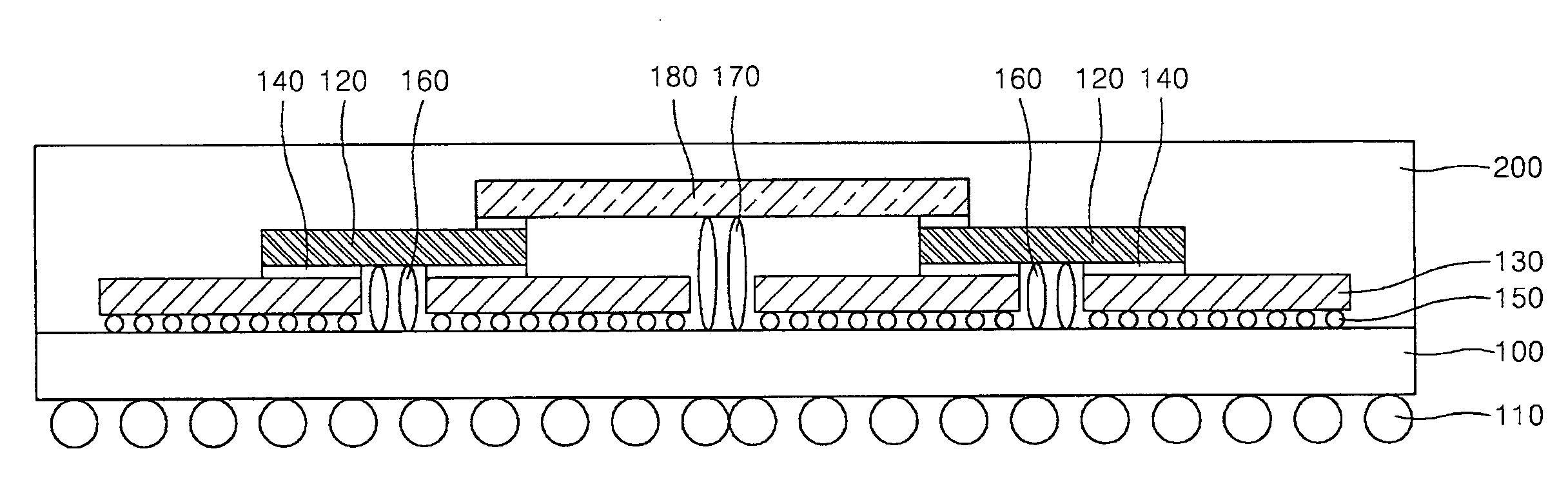
[0055]Embodiments of the present invention will now be described more fully hereinafter with reference to the accompanying drawings, in which preferred embodiments of the invention are shown. This invention may, however, be embodied in different forms and should not be construed as limited to the embodiments set forth herein. Like numbers refer to like elements throughout the specification.

[0056]It will be understood that, although the terms first, second, etc. are used herein to describe various elements, these elements should not be limited by these terms. These terms are used to distinguish one element from another. For example, a first element could be termed a second element, and, similarly, a second element could be termed a first element, without departing from the scope of the present invention. As used herein, the term “and / or” includes any and all combinations of one or more of the associated listed items.

[0057]It will be understood that when an element is referred to as b...


PUM


Abstract

In a semiconductor device stack package and a method of forming the same, the package comprises: a substrate; a plurality of lower chips stacked on the substrate and having an active surface oriented in a direction toward the substrate; and at least one upper chip disposed on the lower chips and connected to the substrate via a bump disposed between the lower chips. As no wire loops are formed, there is no increase in the height of the stack package, and the electrical path is shortened, thereby improving the electric performance of the stack package. Also, the semiconductor device stack package has a flip chip structure, and thus a plurality of semiconductor chips can be stacked in various manners.

Description

CROSS-REFERENCE TO RELATED PATENT APPLICATION[0001]This application claims the benefit of Korean Patent Application No. 10-2007-0038326, filed on Apr. 19, 2007, in the Korean Intellectual Property Office, the disclosure of which is incorporated herein in its entirety by reference.BACKGROUND OF THE INVENTION[0002]1. Field of the Invention[0003]Embodiments of the present invention relate to a semiconductor device stack package, an electronic apparatus including the same, and a manufacturing method of the semiconductor device stack package, and more particularly, to a stack package in which an active surface of an upper chip is oriented toward a substrate and the upper chip is connected via a bump-type interconnect to the substrate, an electronic apparatus including the stack package, and a manufacturing method of the semiconductor device stack package.[0004]2. Description of the Related Art[0005]In general, a plurality of semiconductor chips are commonly formed on a semiconductor subs...

Claims


Application Information

Patent Timeline
Patent Type & Authority Applications(United States)
IPC IPC(8): H01L23/48H01L21/50
CPCH01L24/12H01L24/16H01L24/73H01L25/0652H01L2224/13099H01L2224/16225H01L2224/32145H01L2224/32225H01L2224/48091H01L2224/48227H01L2224/83194H01L2225/06517H01L2924/01078H01L2924/15311H01L2924/00014H01L24/32H01L2924/01033H01L2924/014H01L2224/4824H01L2224/73265H01L2924/00H01L2924/181H01L2224/05573H01L2224/13025H01L2224/056H01L2224/0401H01L2224/06134H01L2224/06136H01L2224/16227H01L2224/73203H01L2224/73253H01L2224/0554H01L2924/00012H01L2224/05599H01L2224/0555H01L2224/0556H01L23/12
Inventor PARK, JIN-WOOJO, CHA-JEAHN, EUN-CHULHWANG, TAE-JOOYU, HAE-JUNGPARK, CHAN
Owner SAMSUNG ELECTRONICS CO LTD
Why Eureka
Try Eureka