
Composite transparent conductors and methods of forming the same

a conductor and transparent technology, applied in the field of transparent conductors, can solve the problems of high cost of metal oxide film fabrication, and high optical absorption, and achieve the effect of improving drawing legibility

Active Publication Date: 2008-10-23
CHAMP GREAT INTL
View PDF25 Cites 294 Cited by
  • Summary
  • Abstract
  • Description
  • Claims
  • Application Information

AI Technical Summary

Benefits of technology

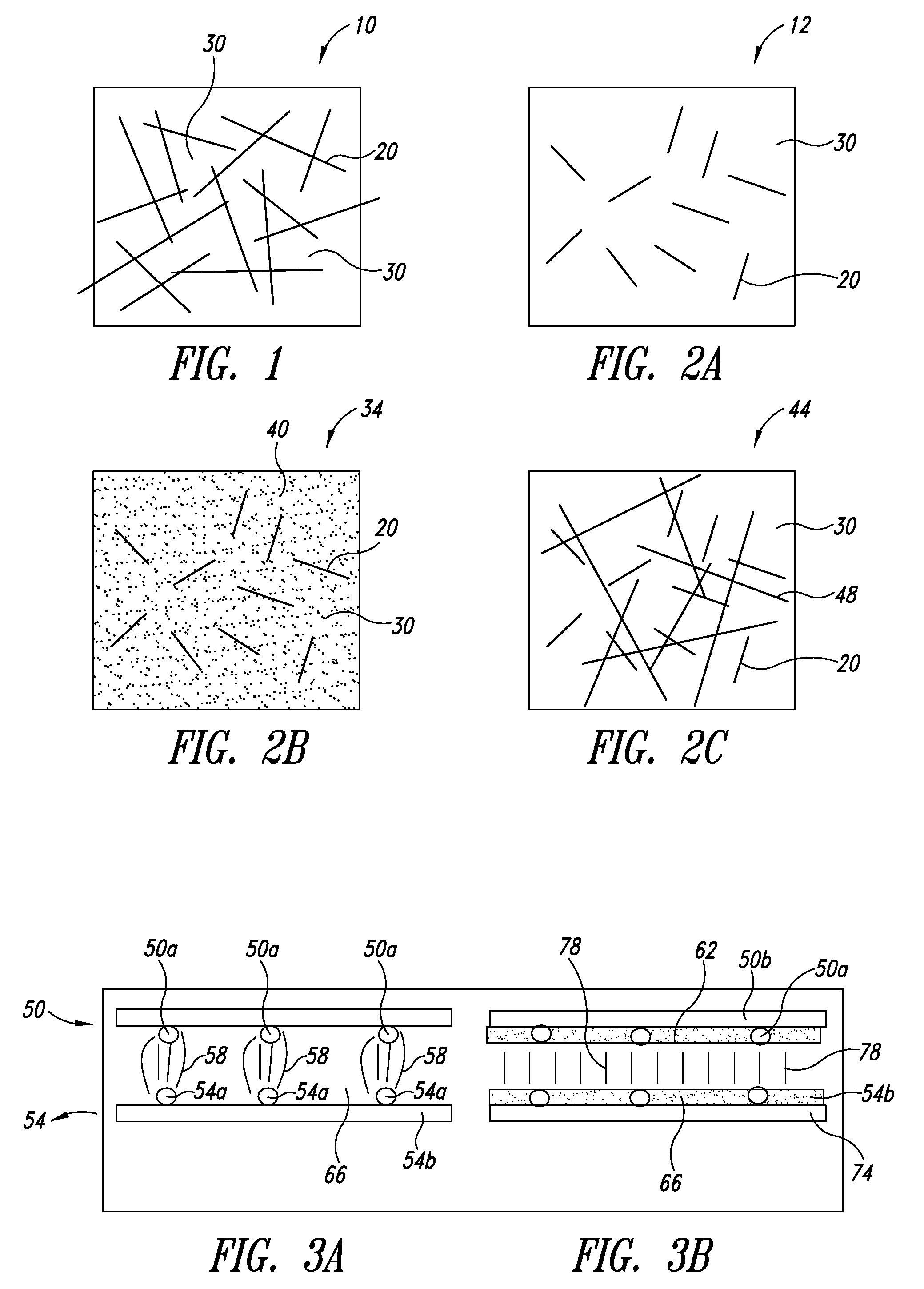
[0014]In the drawings, identical reference numbers identify similar elements or acts. The sizes and relative positions of elements in the drawings are not necessarily drawn to scale. For example, the shapes of various elements and angles are not drawn to scale, and some of these elements are

Problems solved by technology

However, metal oxide films are costly to fabricate because they require vacuum chambers, elevated deposition temperatures and / or high annealing temperatures to achieve high conductivity.
Metal oxide films are also fragile and prone to damage even when subjected to minor physical stresses such as bending.
However, they generally have lower conductivity values and higher optical absorption (particularly at visible wavelengths) compared to the metal oxide films, and suffer from lack of chemical and long-term stability.

Method used


Image

  • Composite transparent conductors and methods of forming the same
  • Composite transparent conductors and methods of forming the same
  • Composite transparent conductors and methods of forming the same

Examples


example 1

Synthesis of Silver Nanowires

[0130]Silver nanowires were synthesized by a reduction of silver nitrate dissolved in ethylene glycol in the presence of poly(vinyl pyrrolidone) (PVP). The method was described in, e.g. Y. Sun, B. Gates, B. Mayers, & Y. Xia, “Crystalline silver nanowires by soft solution processing”, Nanolett, (2002), 2(2) 165-168. Uniform silver nanowires can be selectively isolated by centrifugation or other known methods.

[0131]Alternatively, uniform silver nanowires can be synthesized directly by the addition of a suitable ionic additive (e.g., tetrabutylammonium chloride) to the above reaction mixture. The silver nanowires thus produced can be used directly without a separate step of size-selection. This synthesis is described in more detail in U.S. Provisional Application No. 60 / 815,627, in the name of Cambrios Technologies Corporation, the assignee of the present application, which application is incorporated herein in it entirety.

[0132]In the following examples, ...

example 2

Preparation of Composite Transparent Conductors

[0133]The metal nanowires can be formulated into an ink composition prior to deposition on a substrate or a continuous conductive film such as ITO film, and conductive polymer films.

[0134]An ITO film can be directly sputtered on a substrate followed by the deposition of the nanowire layer. Alternatively, a nanowire layer can be first deposited on a substrate, followed by sputtering an ITO film directly on the nanowire layer.

[0135]If the secondary conductive medium includes carbon nanotubes, the carbon nanotubes can be formulated into the same ink composition with the metal nanowires for co-deposition. Alternatively, the carbon nanotubes can be formulated into a separate ink composition for serial deposition before or after the deposition of the metal nanowires.

[0136]Typically, the ink composition comprises agents that facilitate dispersion of the nanostructures and / or immobilization of the nanostructures on the substrates. These agents...

example 3

Evaluation of Optical and Electrical Properties of Transparent Conductors

[0146]The composite transparent conductors prepared according to the methods described herein were evaluated to establish their optical and electrical properties.

[0147]The light transmission data were obtained according to the methodology in ASTM D1003. Haze was measured using a BYK Gardner Haze-gard Plus. The surface resistivity was measured using a Fluke 175 True RMS Multimeter or contactless resistance meter, Delcom model 717B conductance monitor. A more typical device is a 4 point probe system for measuring resistance (e.g., by Keithley Instruments).

[0148]The interconnectivity of the nanowires and an areal coverage of the substrate can also be observed under an optical or scanning electron microscope.


PUM


Abstract

Composite transparent conductors are described, which comprise a primary conductive medium based on metal nanowires and a secondary conductive medium based on a continuous conductive film.

Description

CROSS-REFERENCE TO RELATED APPLICATIONS[0001]This application claims benefit under 35 U.S.C. 119(e) of U.S. Provisional Patent Application No. 60 / 913,231, filed Apr. 20, 2007, which is incorporated herein by reference in its entirety.BACKGROUND[0002]1. Technical Field[0003]This disclosure is related to composite transparent conductors based on conductive nanostructures, and methods of forming the same.[0004]2. Description of the Related Art[0005]Transparent conductors refer to optically transparent, thin conductive films. They are widely used as transparent electrodes in flat panel electrochomic displays such as liquid crystal displays, plasma displays, touch panels, electroluminescent devices and thin film photovoltaic cells, as anti-static layers and as electromagnetic wave shielding layers.[0006]Conventional transparent conductors include vacuum deposited metal oxides, such as indium tin oxide (ITO). However, metal oxide films are costly to fabricate because they require vacuum c...

Claims


Application Information

Patent Timeline
IPC IPC(8): G02F1/1343H01B5/00
CPCB82Y10/00B82Y30/00G02F1/13439H01L31/1884H01L51/0048H01L51/5206H01L29/413H05K3/245H05K3/249H05K2201/0108H05K2201/026Y02E10/50H01L29/0669H05K1/097H10K85/221H10K50/81H01B5/00G02F1/00
Inventor JONES, DAVIDPSCHENITZKA, FLORIANQUAN, XINASPAID, MICHAEL A.WOLK, JEFFREY
Owner CHAMP GREAT INTL
Learn More