Photomask with detector for optimizing an integrated circuit production process and method of manufacturing an integrated circuit using the same

a technology of integrated circuit and production process, applied in the direction of photomechanical equipment, originals for photomechanical treatment, instruments, etc., can solve the problems of inability to make circuits from photomasks, high cost, and time-consuming process of manufacturing photomasks

Active Publication Date: 2008-10-23
PHOTRONICS INC
View PDF63 Cites 9 Cited by
  • Summary
  • Abstract
  • Description
  • Claims
  • Application Information

AI Technical Summary

Benefits of technology

[0023]According to an exemplary embodiment of the present invention, a photomask for integrated circuit production for development of integrated circuit components, where the integrated circuit production uses a radiation source that generates a source image, comprises: a substrate with one or more layers disposed thereon; a source separator element that separates the source image into one or more duplicate source images; one or more polarizing elements each corresponding to one of the one or more duplicate source images; and one or more sensors each corresponding to one of the one or more polarizing elements, the one or more sensors sensing one or more radiation characteristics of the radiation source.

Problems solved by technology

The process of manufacturing a photomask involves many steps and can be time consuming.
The fracturing process can be very time consuming.
A defect is any flaw affecting the geometry.
This includes undesirable chrome areas (chrome spots, chrome extensions, chrome bridging between geometry) or unwanted clear areas (pin holes, clear extensions, clear breaks).
A defect can cause the circuit to be made from the photomask not to function.
This often requires numerous interruptions of the overall manufacturing process to conduct steps such as simulation of the photomask performance and sampling of the integrated circuit to determine whether adjustments to the process are required.
The time required to sample the integrated circuit and perform other monitoring steps, analyze the results, and make the necessary adjustments to the manufacturing process may result in substantial delays, thereby generating a lower yield and a reduced overall profit margin for the integrated circuit manufacturer.
The photomask is generally considered to be an “unsafe” or “unsecure” medium for electronics design information.
In the extreme case, the device can be fabricated in whole in or in part by an unauthorized source if the masks are in the parties' possession.
However, this protection method cannot prevent unauthorized exposure of the mask or physically secure the content on the mask.
In general, there is no way at present to physically validate and secure the content of a mask at the point of use.

Method used


Image

  • Photomask with detector for optimizing an integrated circuit production process and method of manufacturing an integrated circuit using the same
  • Photomask with detector for optimizing an integrated circuit production process and method of manufacturing an integrated circuit using the same
  • Photomask with detector for optimizing an integrated circuit production process and method of manufacturing an integrated circuit using the same

Examples


Embodiment Construction

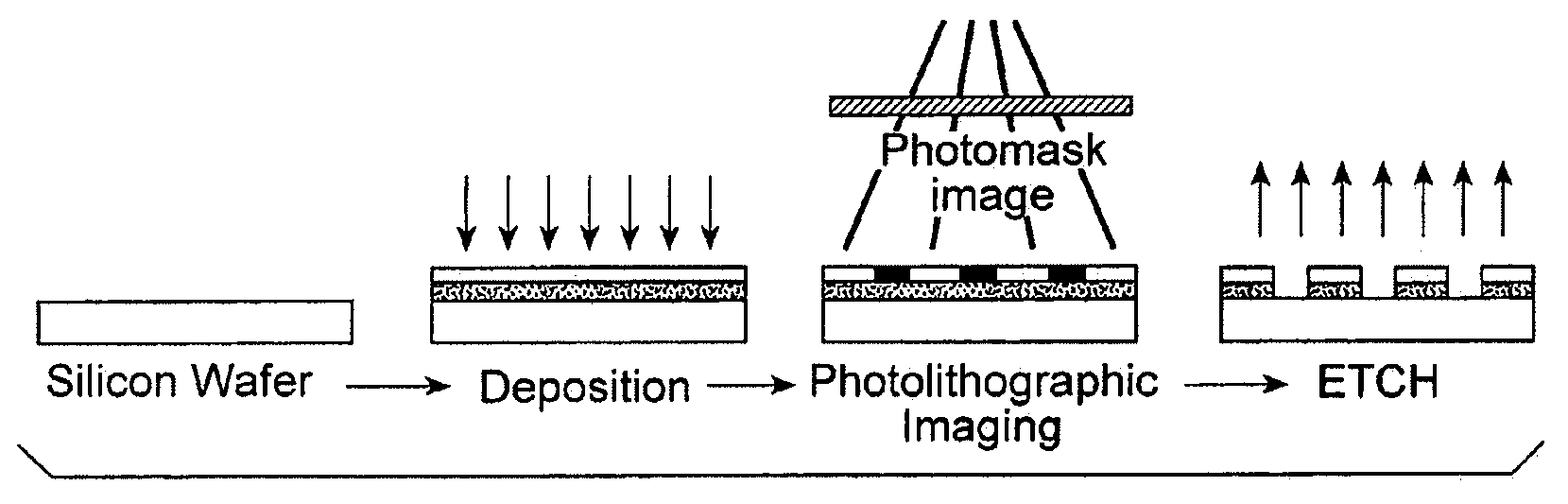
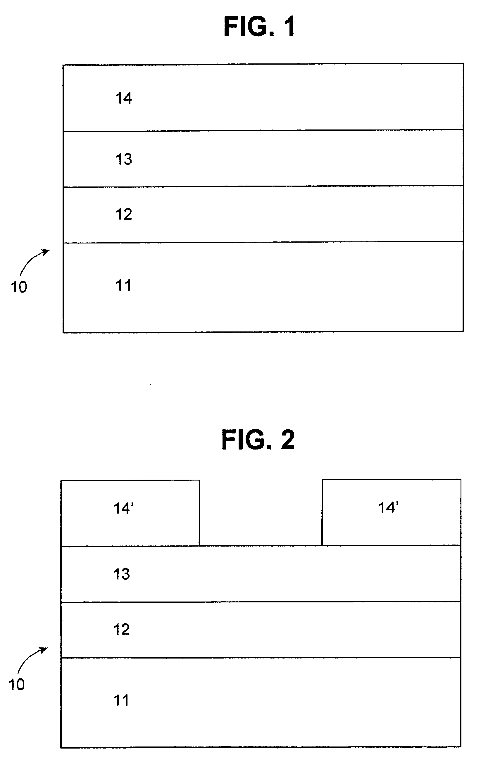
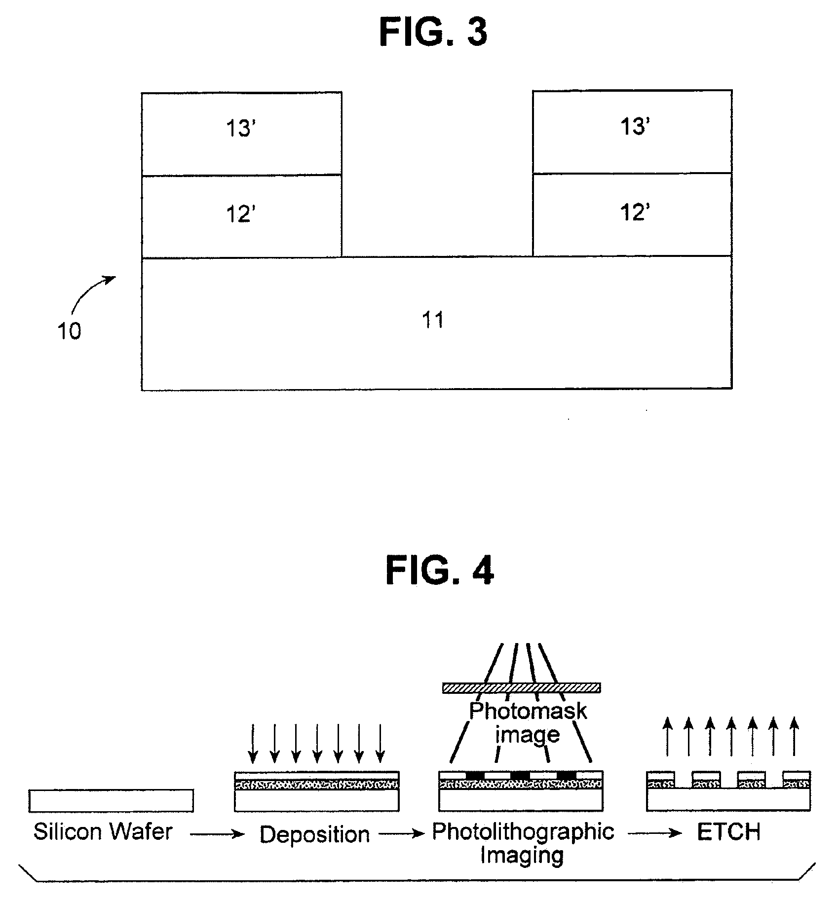
[0055]Various exemplary embodiments of the present invention are directed to a photomask having electronics and detection capability integrated into the photomask substrate to enable wireless or other type of communication of information between the photomask and other elements of mask and wafer manufacturing processes including but not limited to mask making equipment, wafer exposure equipment, design automation tools, simulation tools, process control systems and mask tracking / logistical / shipping systems. The inventive photomask preferably has the ability to detect irradiation used to expose photomasks onto a wafer, such as, for example, 193 nm laser light in a wafer exposure scanner or other appropriate wavelength laser light. As explained in further detail below, such detected information may to be stored and analyzed for improving process capability. Information relevant to the manufacturing of the photomask, such as pattern metrology data, defects, and registration information...


PUM

PropertyMeasurementUnit
wavelengthaaaaaaaaaa
transparentaaaaaaaaaa
antireflectiveaaaaaaaaaa

Abstract

A photomask for integrated circuit production for development of integrated circuit components, where the integrated circuit production uses a radiation source that generates a source image, includes a substrate with one or more layers disposed thereon; a source separator element that separates the source image into one or more duplicate source images; one or more polarizing elements each corresponding to one of the one or more duplicate source images; and one or more sensors each corresponding to one of the one or more polarizing elements, the one or more sensors sensing one or more radiation characteristics of the radiation source.

Description

RELATED APPLICATIONS[0001]This application is a continuation-in-part of U.S. patent application Ser. No. 11 / 788,473, filed Apr. 20, 2007, the contents of which are incorporated herein by reference.FIELD OF THE INVENTION[0002]The present invention generally relates to photomasks and optical lithography for fabrication of integrated circuits. The present invention also generally relates to a method of manufacturing integrated circuits using photomasks.BACKGROUND OF THE INVENTION[0003]Photomasks are high precision plates containing microscopic images of electronic circuits. Photomasks are typically made from very flat pieces of quartz or glass with a layer of chrome on one side. Etched in the chrome is a portion of an electronic circuit design. This circuit design on the mask is also called “geometry.” A typical photomask used in the production of semiconductor devices is formed from a “blank” or “undeveloped” photomask. As shown in FIG. 1, a typical blank photomask 5 is comprised of t...

Claims


Application Information

Patent Timeline
Patent Type & Authority Applications(United States)
IPC IPC(8): G03F1/00G03F7/20
CPCG03F1/14G03F7/70566G03F1/38G03F1/44
Inventor PROGLER, CHRISTOPHER J.
Owner PHOTRONICS INC
Why Eureka
Try Eureka