Substrate and negative imaging method for providing transparent conducting patterns

Inactive Publication Date: 2008-10-30
EI DU PONT DE NEMOURS & CO
View PDF23 Cites 20 Cited by
  • Summary
  • Abstract
  • Description
  • Claims
  • Application Information

AI Technical Summary

Benefits of technology

[0011](c) exposing a portion of the assemblage to an IR light beam to provide an exposed substrate having at least one exposed region, and at least one unexposed region having

Problems solved by technology

The high cost of the fabrication methods and the low flexibility of such electrodes, due to the brittleness of the inorganic ITO layer as well as the glass substrate, limit the range of potential applications.
Although many of these polymers are highly colored and are less suited for transparent conductive layer applications, some of these electronically conductive polymers, such as substituted or unsubstituted pyrrole-containing polymers, substituted or unsubstituted thiophene-containing polymers, and substituted or unsubstituted aniline-containing polymers are transparent and not prohibitively colored, at least when coated in thin layers at moderate coverage.
Although there are known methods to form and pattern electronically conductive polymers, there are so

Method used


Image

  • Substrate and negative imaging method for providing transparent conducting patterns
  • Substrate and negative imaging method for providing transparent conducting patterns

Examples


example 1

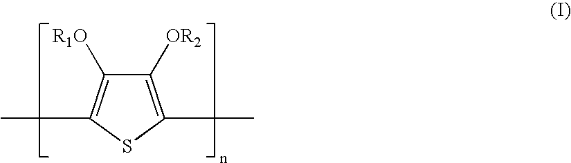
[0107]This example illustrates the formation of a substrate of the invention. The coating composition of Table 1 was coated using a Bushman CN4 coating rod (Bushman Corp., Cleveland Ohio) with a WATERPROOF CV coating system (E.I. DuPont De Nemours, Inc., Wilmington, Del.) onto MELINEX 535 (DuPont-Teijin Films, Hopewell, Va.). The coated base film was dried for 10 min at 45° C. The measured OD at 830 nm was 0.24. The OD throughout the visible range, 400-700 nm, was less than 0.1 at all wavelengths. The thickness of the transparent conducting layer was measured with a Tencor P-15 stylus profilometer (KLA-Tencor, San Jose, Calif.) to be 150 nm. The surface resistance of the conducting layer, was 650 Ohms.

[0108]The peel force for separation of the transparent conducting layer from the base film was measured with an Imass SP-2000 peel tester. The measured peel force was 4300 g per linear inch (1700 g / linear cm) and the failure occurred at the adhesive / glass interface. This demonstrated t...

example 2

[0109]This example illustrates the method for making a transparent conducting pattern.

[0110]The substrate of Example 1 was exposed with near-IR laser light using a CREO Trendsetter exposure unit as described in the methods. The substrate from Example 1 was dried for 60 min at 50° C. The substrate was mounted onto the drum of the exposure unit with the transparent conducting layer facing out from the core of the drum. A receiver consisting of a PET film (2 mil, 0.05 mm) containing Solvent Green 28 dye, as disclosed in the materials section, was loaded second. Films were mounted using vacuum hold down to a standard plastic or metal carrier plate clamped mechanically to the drum. The assemblage was exposed in selected regions at 18 W at 830 nm at a drum speed of 60 rpm from the side through the receiver.

[0111]The pattern that was exposed to the imaging laser consisted of a contiguous exposed region such that the unexposed regions comprised a set of about 50 lines that were 1 mm wide by...

example 3

[0112]This example illustrates the method for making a patterned substrate having a transparent conducting pattern and a second conducting pattern.

[0113]A metal composition comprising Ag flake was first prepared using the materials listed in Table 2. The composition was mixed in a vial with an ultrasound probe (Dukane Co., Model 40TP2000, Transducer Model 41C28) for 15 min, during which the mixture was stirred with a spatula at 5 min intervals. The vial was placed in a water bath with sonication for 1 h, during which the mixture was stirred with a spatula at 0.5 h intervals. The mixture was then treated in a water bath at RT with probe sonication for an additional 15 min, during which the mixture was stirred with a spatula at 5 min intervals. The resulting dispersion was filtered twice through an 8 micron stainless steel screen (Twill Dutch Weave 325×2300, Sefar America Inc.).

TABLE 2Metal Composition for Metal Transfer LayerMaterialWeight (g)SF 69 flake Ag24.015DI water12.7JONCRYL 5...


PUM


Abstract

Provided are processes for making a transparent conducting pattern. The invention is also directed to electronic devices containing such transparent conducting patterns. Further provided is a substrate comprising a base film and a transparent conducting layer disposed on the base film; wherein the substrate has an OD of about 0.1 to 0.6 at 830 nm, and the transparent conducting layer comprises polyethylene dioxythiophene and has an OD of less than 0.1 in the range of 400 to 700 nm.

Description

FIELD OF INVENTION[0001]The invention relates to substrates and processes for providing transparent conducting patterns for electrical applications.BACKGROUND[0002]Transparent electrically-conductive layers of metal oxides such as indium tin oxide (ITO), antimony doped tin oxide, and cadmium stannate (cadmium tin oxide) are commonly used in the manufacture of electrooptical display devices such as liquid crystal display devices (LCDs), electroluminescent display devices, photocells, solid-state image sensors, electrochromic windows and the like.[0003]Devices such as flat panel displays typically contain a substrate provided with an indium tin oxide (ITO) layer as a transparent electrode. The coating of ITO is carried out by vacuum sputtering methods which involve high substrate temperature conditions up to 250° C., and therefore, glass substrates are generally used. The high cost of the fabrication methods and the low flexibility of such electrodes, due to the brittleness of the ino...

Claims


Application Information

Patent Timeline
IPC IPC(8): H05K1/09
CPCH01L31/1884H01L51/0013H01L51/0021H01L51/0023H01L51/0096H05K3/046H05K2201/0108H05K2201/0329H05K2203/0528H05K2203/107Y02E10/549Y02P70/50H10K71/18H10K71/60H10K71/621H10K77/10
Inventor CATRON, JOHNGAO, FENGJOHNSON, LYNDA KAYEMETH, JEFFREY SCOTTZANE, STEPHEN G.
Owner EI DU PONT DE NEMOURS & CO
Why Eureka
Try Eureka