Capacitor Devices

a technology of capacitors and devices, applied in the field of capacitors, can solve the problems of reducing the thickness of the dielectric layer, presenting difficulties, and limiting the selection of dielectric materials

Active Publication Date: 2008-10-30
IND TECH RES INST
View PDF10 Cites 40 Cited by
  • Summary
  • Abstract
  • Description
  • Claims
  • Application Information

AI Technical Summary

Problems solved by technology

However, each of these approaches presents difficulties.
First, increasing the area of the conducting plates departs from the object of compact designs.
In addition, the selection of the dielectric material is often limited by many production and configuration limitations.
Additional difficulties arise when the thickness of a dielectric layer is reduced.
In particular, the thickness of a dielectric layer on a circuit board can be difficult to control because dielectric thickness may be dramatically changed due to the shapes and dimensions of the patterned features (e.g., capacitor electrodes) over which dielectric is deposited.
A thin-dielectric layer design usually comes with the danger of having metal-to-metal shorting through the thin dielectric layer and of having microscopic voids or other structural defects in the layer that may impact capacitive effects and characteristics.

Method used


Image

  • Capacitor Devices
  • Capacitor Devices
  • Capacitor Devices

Examples


Embodiment Construction

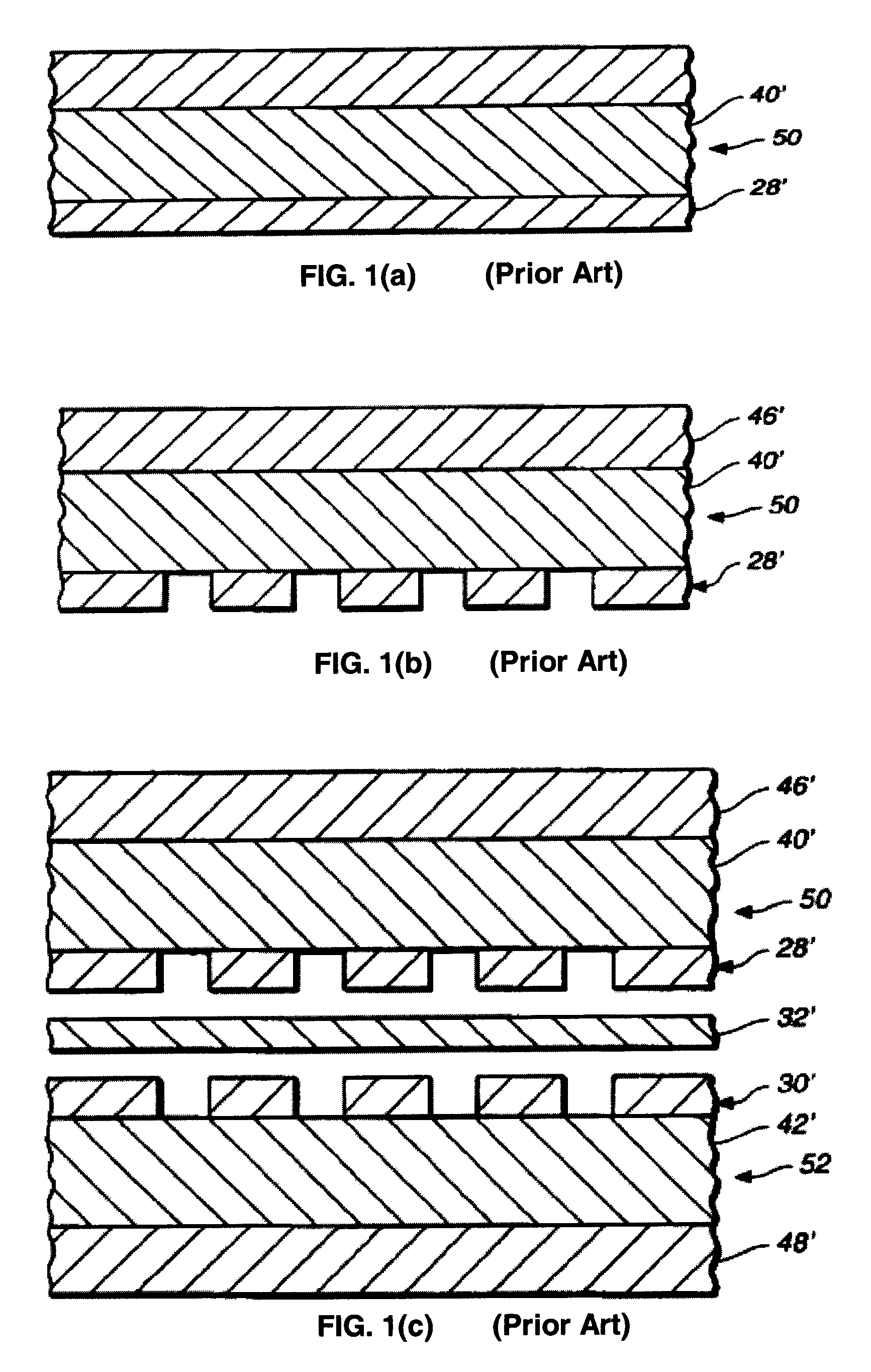
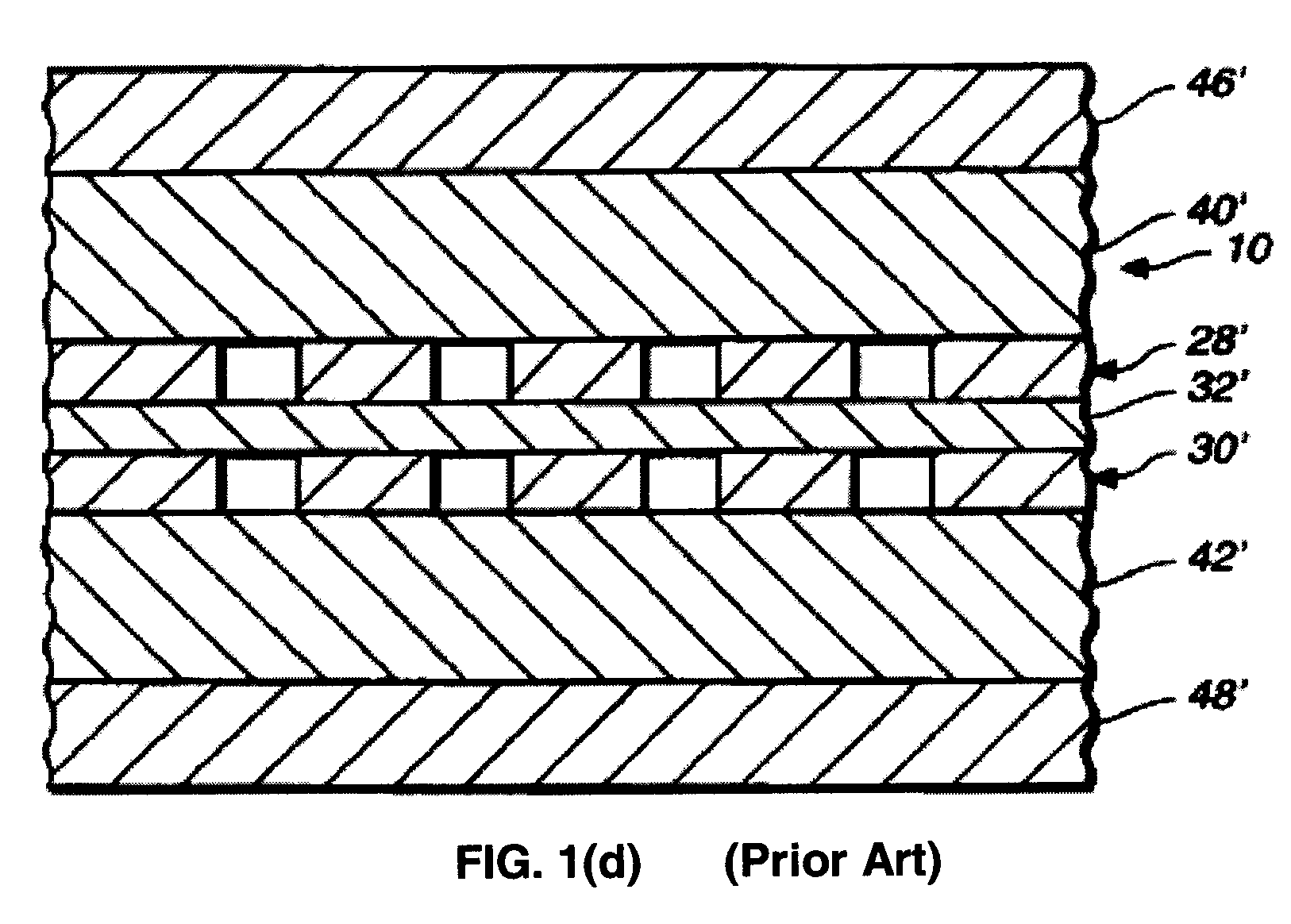
[0030]U.S. Pat. No. 5,800,575 describes one method of fabricating a metal-insulator-metal (MIM) capacitor. Referring to FIG. 1(a), the fabrication process may start from forming an initial lamination product 50 which includes the fully cured dielectric sheet 40′ with conductive foils 28′ and 46′ laminated or bonded on opposite sides of the dielectric sheet 40′. Thereafter, the conductive foil 28′ is etched as indicated in FIG. 1 (b). Referring to FIG. 1(c), another lamination product 52 is formed in a similar manner as the lamination product 50. The lamination product 52 includes the other dielectric layer 42′ and the conductive foils 30′ and 48′. An uncured dielectric sheet 32′ is then arranged between the lamination products 50 and 52 so that it is adjacent to both the conductive foils 28′ and 30′. After a conventional lamination to convert the uncured dielectric sheet 32′ to a fully cured condition, the finished capacitive PCB 10′ is formed as shown in FIG. 1(d). The thickness of...


PUM

PropertyMeasurementUnit
thicknessaaaaaaaaaa
thicknessaaaaaaaaaa
thicknessaaaaaaaaaa

Abstract

A capacitor device with a capacitance is introduced. The capacitor device includes at least one capacitive element. The at least capacitive element comprises a pair of first conductive layers being opposed to each other, at least one first dielectric layer formed on a surface of at least one of the first conductive layers, and a second dielectric layer being sandwiched between the first conductive layers. The first dielectric layer has a first dielectric constant and the second dielectric layer has a second dielectric constant. The capacitance of the capacitor device depends on dielectric parameters of the first dielectric layer and the second dielectric layer. The dielectric parameters comprise the first dielectric constant and thickness of the at least one first dielectric layer and the second dielectric constant and thickness of the second dielectric layer.

Description

BACKGROUND OF THE INVENTION[0001]1. Field of the Invention[0002]This invention generally relates to capacitors, and more particularly, to capacitors that may be embedded within printed circuit boards or other microelectronic devices.[0003]2. Background of the Invention[0004]Capacitors are devices used for introducing capacitance into a circuit. Capacitors function primarily to store electrical energy, block the flow of direct current, or permit the flow of alternating current. They comprise a layer of dielectric material sandwiched between a pair of spaced conductive metal layers, such as copper foils.[0005]Capacitors are common elements on printed circuit boards (PCBs) and other microelectronic devices. In recent years, substantial efforts have been expended in the design of such PCBs and devices arranged thereupon to compensate for voltage fluctuations arising between the power and ground planes in the PCBs. One common type of voltage fluctuations include “switching noises,” which...

Claims


Application Information

Patent Timeline
Patent Type & Authority Applications(United States)
IPC IPC(8): H01G4/06H01G9/00H01G4/12H01G4/20H01G4/33
CPCH01G4/06H01G4/12H01G4/1227H01G4/14H01G4/20H01G4/206Y10T29/417H05K3/4611H05K2201/0187H05K2201/0195H05K2201/09672H05K2201/2036H05K1/162H01L27/04
Inventor WU, SHIH-HSIENLAI, SHINN-JUHLEE, MIN-LINLIU, SHUR-FEN
Owner IND TECH RES INST
Why Eureka
Try Eureka