Method for applying a stress layer to a semiconductor device and device formed therefrom

a stress layer and semiconductor technology, applied in the field of semiconductor devices, can solve the problems of significant limitations in the size and operation speed of such devices, and achieve the effect of reducing power consumption and increasing operating speed

Inactive Publication Date: 2008-11-06
MIE FUJITSU SEMICON
View PDF16 Cites 41 Cited by
  • Summary
  • Abstract
  • Description
  • Claims
  • Application Information

AI Technical Summary

Benefits of technology

[0006]Technical advantages of certain embodiments of the present invention include providing a semiconductor device with increased operating speed and reduced power consumption. Other technical advantages of the present invention will be readily apparent to one skilled in the art from the followi...

Problems solved by technology

With the demand for electronic devices that are increasingly smaller and faster, the inclusion of the metal oxide layer from wh...

Method used


Image

  • Method for applying a stress layer to a semiconductor device and device formed therefrom
  • Method for applying a stress layer to a semiconductor device and device formed therefrom
  • Method for applying a stress layer to a semiconductor device and device formed therefrom

Examples


Embodiment Construction

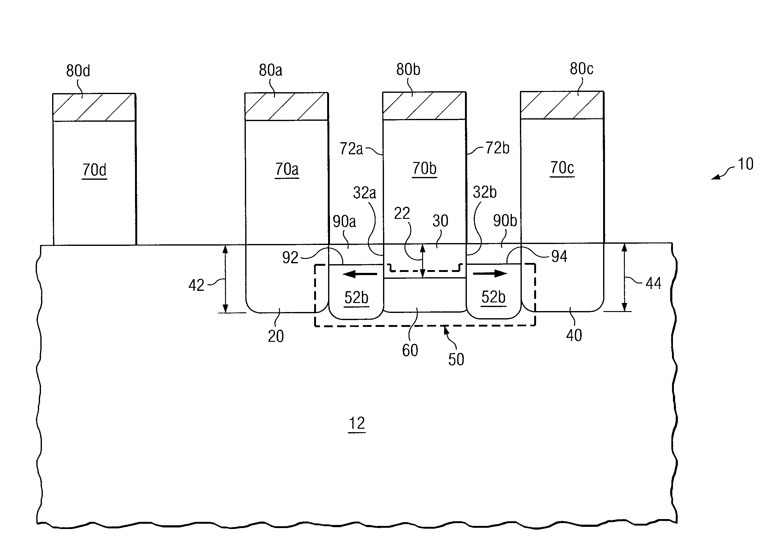
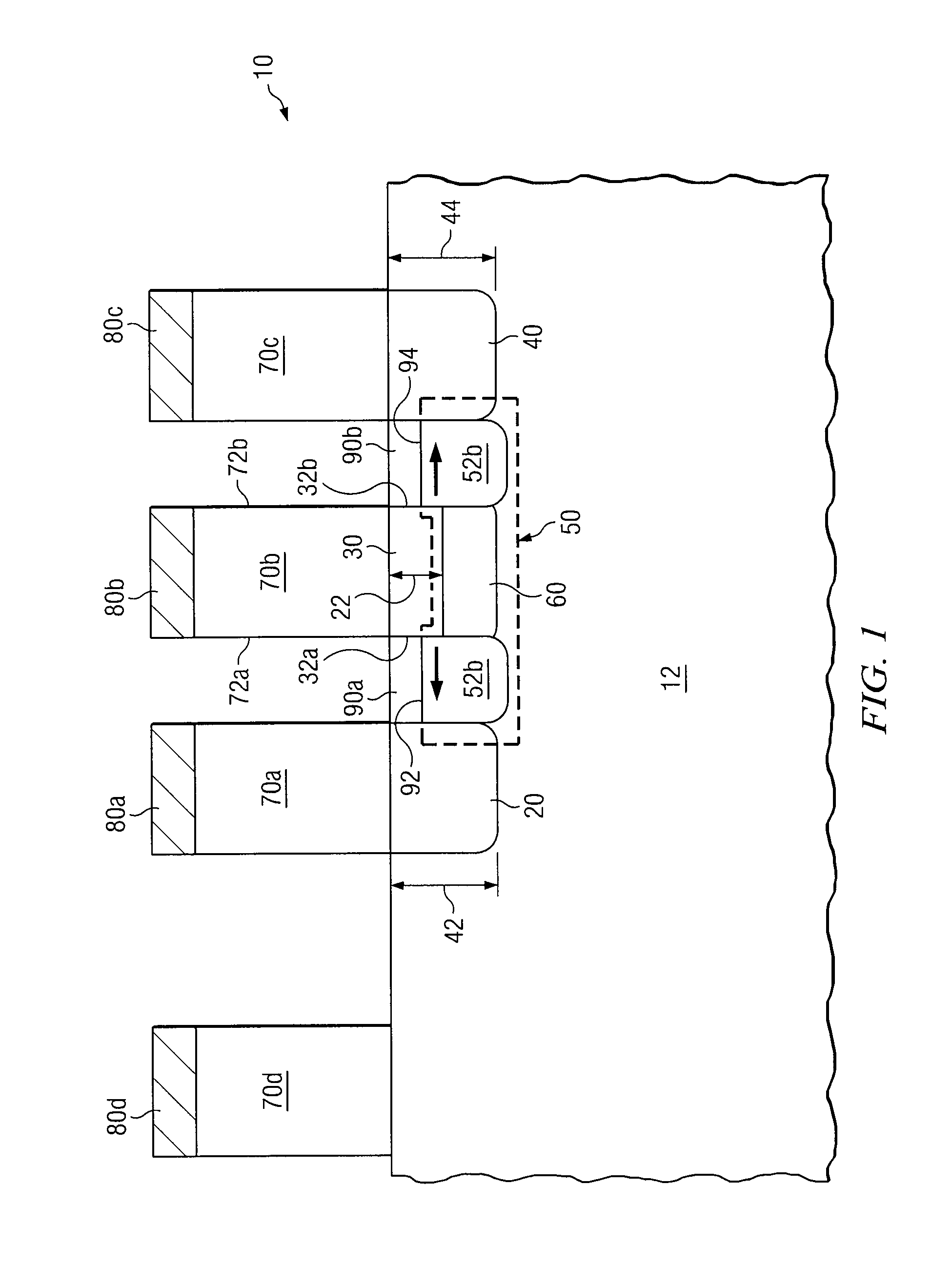
[0010]FIG. 1 shows a cross-sectional view of a semiconductor device 10 according to a particular embodiment of the present invention. As shown in FIG. 1, semiconductor device 10 includes a substrate 12, a source region 20, a gate region 30, a drain region 40, a conducting region 50, polysilicon regions 70a-d, and contacts 80a-d. Additionally, conducting region 50 includes link regions 52a-b and a channel region 60. In general, voltages applied to contacts 80a-d of semiconductor device 10 affect the conductivity of channel region 60 and, when appropriate voltages are applied to contacts 80a-d, a current flows between source region 20 and drain region 40 through conducting region 50. While semiconductor device 10 may represent any appropriate form of electronic device that has the described structure and / or provides the described functionality, in particular embodiments, semiconductor device 10 represents a junction field-effect transistor (JFET).

[0011]As discussed in more detail belo...


PUM


Abstract

A semiconductor device includes a substrate of semiconductor material. A source region, a drain region, and a conducting region of the semiconductor device are formed in the substrate and doped with a first type of impurities. The conducting region is operable to conduct current between the drain region and the source region when the semiconductor device is operating in an on state. A gate region is also formed in the substrate and doped with a second type of impurities. The gate region abuts a channel region of the conducting region. A stress layer is deposited on at least a portion of the conducting region. The stress layer applies a stress to the conducting region along a boundary of the conducting region that strains at least a portion of the conducting region.

Description

TECHNICAL FIELD OF THE INVENTION[0001]This invention relates, in general, to semiconductor devices and, more particularly, to devices utilizing strained semiconductor material.BACKGROUND OF THE INVENTION[0002]As a result of the rapid technological growth of the past several decades, transistors and other semiconductor devices have become a fundamental building block for a wide range electronic components. Metal-oxide silicon field-effect transistors (MOSFET) have been the primary choice for transistors in many applications including general-use microprocessors, digital signal processors, application specific integrated circuits (ASICs) and various other forms of electronic devices. With the demand for electronic devices that are increasingly smaller and faster, the inclusion of the metal oxide layer from which MOSFETs derive their name creates significant limitations to further improvements in the size and operating speed of such devices.[0003]As a result, the focus of industry deve...

Claims


Application Information

Patent Timeline
IPC IPC(8): H01L21/337H01L29/80
CPCH01L29/66901H01L29/808H01L29/0653
Inventor KAPOOR, ASHOK K.
Owner MIE FUJITSU SEMICON
Why Eureka
Try Eureka