Dual substrate orientation or bulk on SOI integrations using oxidation for silicon epitaxy spacer formation

a technology of silicon epitaxy and integration, which is applied in the field of high-performance complementary metal oxide semiconductor (cmos) field effect transistors (fets) fabrication, can solve problems such as increasing integration complexity

Active Publication Date: 2008-11-06
NXP USA INC
View PDF16 Cites 61 Cited by
  • Summary
  • Abstract
  • Description
  • Claims
  • Application Information

AI Technical Summary

Problems solved by technology

However, the presence of the nitride sidewall spacers 9 can result in increased integration complexity

Method used


Image

  • Dual substrate orientation or bulk on SOI integrations using oxidation for silicon epitaxy spacer formation
  • Dual substrate orientation or bulk on SOI integrations using oxidation for silicon epitaxy spacer formation
  • Dual substrate orientation or bulk on SOI integrations using oxidation for silicon epitaxy spacer formation

Examples


Embodiment Construction

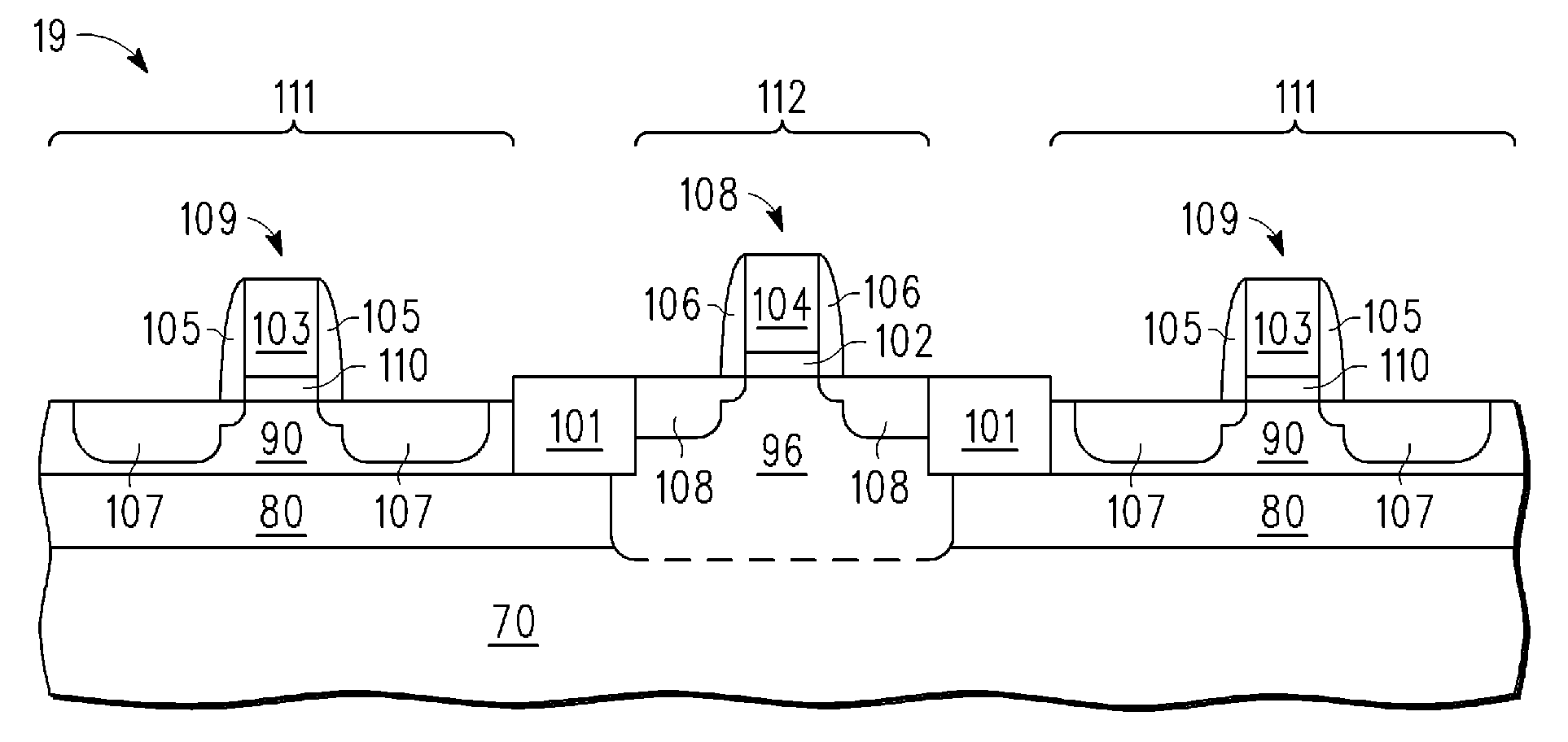
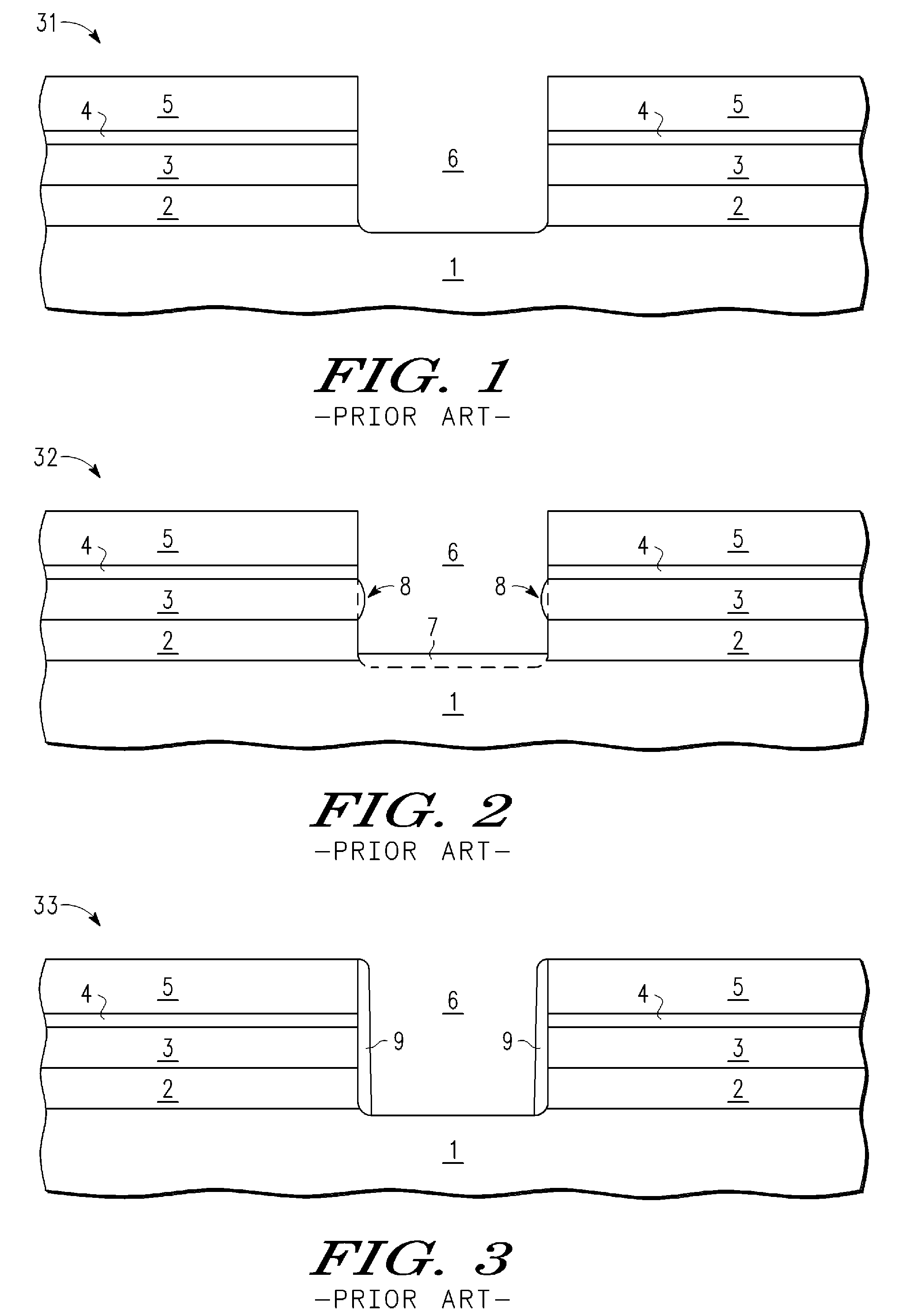
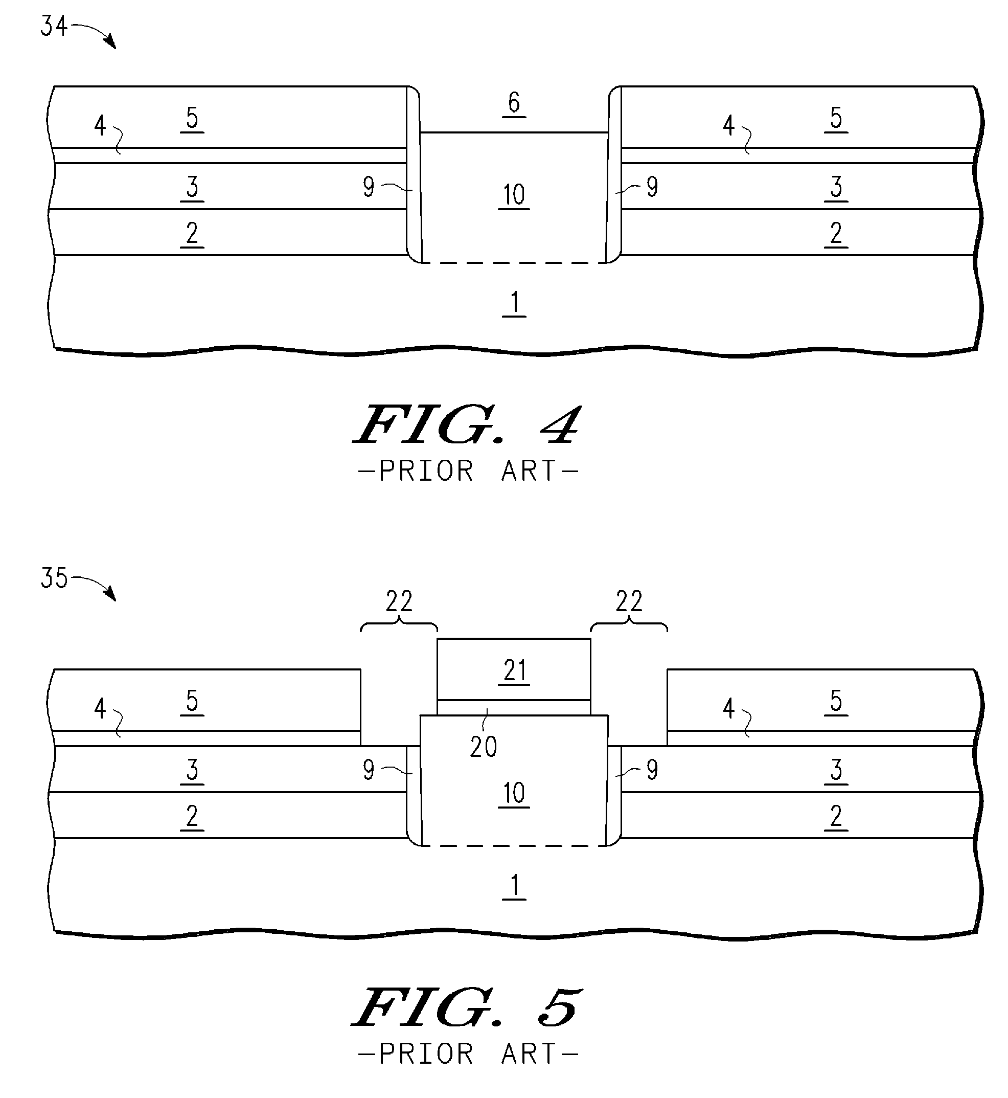
[0023]A method and apparatus are described for fabricating high performance CMOS devices with hybrid substrates by oxidizing SOI sidewalls in a trench opening to form SOI sidewall oxide spacers for DSO and BOS selective epitaxial silicon growth. As a preliminary matter, SOI sidewall oxide spacers are formed in a trench opening, such as by applying a thermal oxidation process which converts the SOI semiconductor layer to an oxide, e.g., silicon dioxide. After formation of the SOI sidewall oxide spacers, a buried oxide etch process simultaneously trims the SOI sidewall oxide spacers while extending the trench opening through a buried oxide layer to expose the underlying bulk substrate for subsequent epitaxial growth. In this way, SOI sidewall spacers are formed that prevent epitaxial growth on the SOI sidewalls in the trench opening during the epitaxial growth step. These sidewall spacers can be readily removed during any subsequent STI etch process without requiring any complex STI e...


PUM


Abstract

A semiconductor process and apparatus provide a planarized hybrid substrate (15) by thermally oxidizing SOI sidewalls (90) in a trench opening (93) to form SOI sidewall oxide spacers (94) which are trimmed while etching through a buried oxide layer (80) to expose the underlying bulk substrate (70) for subsequent epitaxial growth of an epitaxial semiconductor layer (96). In this way, SOI sidewall oxide spacers (94) are formed that prevent epitaxial SOI sidewalls from being formed in the trench opening (93) during the epitaxial growth step, and that can be readily removed during any subsequent STI etch process

Description

BACKGROUND OF THE INVENTION[0001]1. Field of the Invention[0002]The present invention is directed in general to the field of semiconductor devices. In one aspect, the present invention relates to high-performance complementary metal oxide semiconductor (CMOS) field effect transistors (FETs) fabricated on epitaxially grown substrates.[0003]2. Description of the Related Art[0004]To address the difference in electron and hole mobility values for NMOS and PMOS transistor devices formed on semiconductor wafers having a single crystal orientation, CMOS devices are increasingly fabricated with hybrid substrates with different surface orientations that are formed using Dual Substrate Orientation (DSO) integrations. Such hybrid substrates provide PMOS and NMOS devices with their own optimized crystal orientation. In addition, while some devices exhibit performance improvement from being fabricated on semiconductor-on-insulator (SOI) substrates, others benefit from being fabricated on bulk su...

Claims


Application Information

Patent Timeline
IPC IPC(8): H01L21/8238
CPCH01L21/76283H01L21/823807H01L27/1207H01L21/84H01L27/1203H01L21/823878
Inventor SPENCER, GREGORY S.GRANT, JOHN M.KARVE, GAURI V.
Owner NXP USA INC
Why Eureka
Try Eureka