Multi-layer printed circuit board and method of manufacturing multilayer printed circuit board

a printed circuit board and multi-layer technology, applied in the direction of conductive pattern formation, insulating substrate metal adhesion improvement, electric connection formation of printed elements, etc., can solve the problems of deteriorating reliability of printed circuit board connection, inability to form fine through holes, and inability to meet the requirements of reliability, so as to shorten the time required for forming openings.

Inactive Publication Date: 2008-11-13
IBIDEN CO LTD
View PDF32 Cites 44 Cited by
  • Summary
  • Abstract
  • Description
  • Claims
  • Application Information

AI Technical Summary

Benefits of technology

[0025]Multi-layer printed circuit boards claimed in claims 1 and 2 and a method of manufacturing a multi-layer printed circuit board claimed in claim 3 are arranged to maintain required strength of a core substrate thereof by sandwiching a metal layer by resin. Thus, the thickness of the core substrate can be reduced. Hence it follows that the thickness of the multi-layer printed circuit board can be reduced. Since non-penetrating openings which reach the metal layer are simply required to be formed in the resin layer, the depth of each of penetrating openings which are formed by laser beams can be reduced to half or smaller as compared with the conventional core substrate. Therefore, fine non-penetrating openings can easily be formed by laser beams and, therefore, through holes each having a small diameter can be formed. As a result, a degree of integration of the multi-layer printed circuit board can be raised. Moreover, the core substrate is formed into the multilayer structure and, therefore, the metal layer between resin portions which constitute the core substrate permits wiring to be arranged. As a result, the number of layers of the multi-layer printed circuit board can be reduced. Since the non-penetrating openings are filled with plating, the intensity increases and the warpage does not easily occur.
[0095]A printed circuit board and a method of manufacturing a printed circuit board claimed in claims 23 to 26 have a structure that the resin plate has openings formed by CO2 laser beams (YAG laser beams, excimer laser beams or UV laser beams). Therefore, penetrating openings each having a smaller diameter as compared with that of each of penetrating openings formed by drilling can be formed. As distinct from a structure that openings are formed in a copper-clad laminated board by laser beams, leaving of copper in the through hole which causes a plated film formed in the through hole to be separated can be prevented. Moreover, time required to form the openings can be shortened. The openings are formed in the resin plate by using laser beams, and then one or more elements selected from Cu, Ni, Cr, Pd and Mo is brought into contact with the resin. Therefore, strength between the sputtered layer and the resin of 1.0 kg / cm2 can be realized which is substantially the same as that realized by the conventional copper-clad laminated board.

Problems solved by technology

Since the core substrate has a thickness of about 1 mm, fine through holes cannot, however, easily be formed.
Thus, satisfactory reliability cannot be obtained.
Thus, a fact has been detected that the reliability in the connection of the printed circuit board deteriorates owing to the air bubble and the non-filled portion.
Thus, the process takes a long time and the cost is enlarged.
A fact has, however, been detected that the BT resin board having a flat surface encounters deterioration in the adhesiveness with a metal film formed on the right side of the core substrate.
Thus, there arises problems in that the resin film, however, encounters decrease in the strength required for the core substrate and the interlayer resin insulating layer cannot be formed in the upper layer.
To form hundreds of through holes, an excessively long machining time is required and the manufacturing cost cannot be reduced.
Therefore, satisfactory reliability cannot be realized as compared with conventional through holes formed by drilling and each having a large diameter.
When the penetrating openings are formed in a copper-clad laminated board employed to serve as the core substrate, the number of laser shots are increased excessively and an excessively long time is required.
When the openings are formed by the laser beams, a portion of copper for forming copper foil on the surface of the inner wall of the through hole is undesirably left.
It leads to a fact that undesirable separation of the plated film formed in the through hole takes place.

Method used


Image

  • Multi-layer printed circuit board and method of manufacturing multilayer printed circuit board
  • Multi-layer printed circuit board and method of manufacturing multilayer printed circuit board
  • Multi-layer printed circuit board and method of manufacturing multilayer printed circuit board

Examples


first embodiment

(Fourth Modification of First Embodiment)

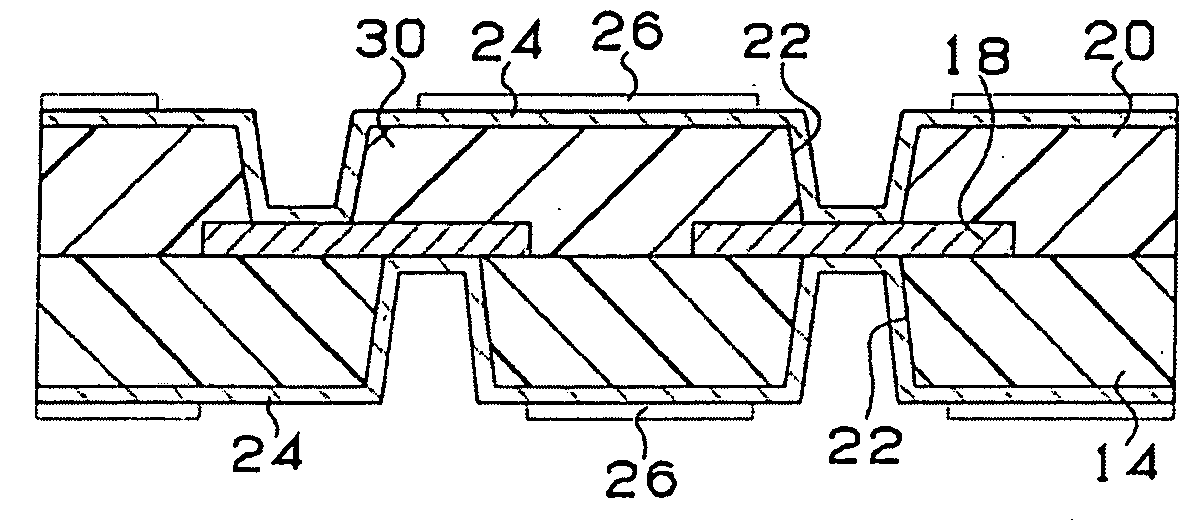
[0225]The structure of a multi-layer printed circuit board according to a fourth modification of the first embodiment will now be described with reference to FIG. 11.

[0226]The multi-layer printed circuit board according to the first embodiment described with reference to FIG. 6 incorporates the solder bumps 68 for connecting a daughter board, the solder bumps 68 being disposed on the lower surface of the multi-layer printed circuit board.

[0227]On the other hand, the fourth modification incorporates conductive connection pins 78. Since the other structure is similar to that of the multi-layer printed circuit board described with reference to FIG. 6, the other structure is omitted from description.

Second Embodiment

[0228]The structure of the multi-layer printed circuit board according to a second embodiment of the present invention will now be described with reference to FIG. 18 which is a cross sectional view.

[0229]A multi-layer printed circuit...

second embodiment

(Second Modification of Second Embodiment)

[0280]The cross section of a multi-layer printed circuit board according to a second modification is shown in FIG. 24. The structure of the second modification is similar to that according to the second embodiment. Note that the multi-layer printed circuit board according to the second modification has the structure that the interlayer resin insulating layer 250 and the interlayer resin insulating layer 281 are constituted by adhesive agent 257 for the upper layer and adhesive agent 255 for the lower layer each having the following composition. Moreover, coating in the liquid state is Performed, and then exposure and development were performed to form the openings.

[0281]A. Raw Material Composition for Preparing Adhesive Agent for Electroless Plating (Adhesive Agent for Upper Layer)

[Resin Composition (1)]

[0282]Mixing and stirring of 35 parts by weight of resin solution obtained by dissolving 25% acryl material of cresol novolac epoxy resin (m...

third embodiment

(First Modification of Third Embodiment)

[0321]A printed circuit board 320 according to a first modification of the third embodiment will now be described with reference to FIG. 39. In the third embodiment, the BGA is provided. The first modification has a structure similar to that according to the third embodiment. As shown in FIG. 39, a PGA method is employed with which connection is established through conductive connection pins 396 as shown in FIG. 39.

[0322]A method of manufacturing the printed circuit board according to the first modification of the present invention will now be described. When the printed circuit board according to the first modification is manufactured, the following materials are employed. A. a raw material composition (an adhesive agent for the upper layer) for preparing an adhesive agent for electroless plating and B. a raw material composition (an adhesive agent for the lower layer) for preparing the resin insulating agent are similar to those according to...


PUM

PropertyMeasurementUnit
thicknessaaaaaaaaaa
diameteraaaaaaaaaa
thicknessaaaaaaaaaa

Abstract

A metal layer 18 is sandwiched between insulating layers 14 and 20 so that required strength is maintained. Hence it follows that the thickness of a core substrate 30 can be reduced and, therefore, the thickness of a multi-layer printed circuit board can be reduced. Formation of non-penetrating openings 22 which reach the metal layer 18 in the insulating layers 14 and 20 is simply required. Therefore, small non-penetrating openings 22 can easily be formed by applying laser beams. Thus, through holes 36 each having a small diameter can be formed.

Description

CROSS-REFERENCE TO RELATED APPLICATIONS[0001]This application is a continuation of and claims the benefit of priority under 35 U.S.C. §120 from U.S. Ser. No. 10 / 921,525, filed Aug. 19, 2004, which is a divisional of U.S. Ser. No. 09 / 979,388, filed Dec. 28, 2001 and a National Stage 35 USC 371, of International Patent Application PCT / JP00 / 03377, filed May 25, 2000.TECHNICAL FIELD[0002]The present invention relates to a multilayer printed circuit board which can be employed as a package substrate on which electronic elements, such as IC, are mounted. More particularly, the present invention relates to a multi-layer printed circuit board constituted by building interlayer resin insulating layers up on a core substrate and a method of manufacturing a multi-layer printed circuit board.BACKGROUND ART[0003]Hitherto, a buildup multi-layer printed circuit board has been manufactured by a method disclosed in Japanese Patent Laid-Open No. 9-130050.[0004]That is, an interlayer resin insulating ...

Claims


Application Information

Patent Timeline
Patent Type & Authority Applications(United States)
IPC IPC(8): H05K1/02H01L21/48H01L23/498H05K1/03H05K3/00H05K3/10H05K3/18H05K3/38H05K3/42H05K3/46
CPCH05K3/181Y10T29/49155H05K3/385H05K3/387H05K3/388H05K3/423H05K3/426H05K3/427H05K3/4602H05K2201/0195H05K2201/0352H05K2201/0355H05K2201/0394H05K2201/09536H05K2201/09563H05K2201/0959H05K2201/096H05K2201/09736H05K2201/09881H05K2203/0315H05K2203/0733H05K2203/0773H05K2203/1476H01L21/486H01L23/49822H01L23/49827H01L2224/16H01L2924/0102H01L2924/01046H01L2924/01078H01L2924/01079H01L2924/15174H01L2924/15311H01L2924/15312H05K1/036H05K3/0032H05K3/0035H05K3/0038H05K3/108H01L2924/01019H01L2924/01087H01L2224/16235Y10T29/49165Y10T29/49144Y10T29/49126H05K3/381H01L2224/05568H01L2224/05573H01L2224/16225H01L2924/00014H01L2224/05599
Inventor ASAI, MOTOOWANG, DONGDONGMORI, TAKAHIRO
Owner IBIDEN CO LTD
Why Eureka
Try Eureka