

Wiring board with built-in component and method for manufacturing the same
- Summary
- Abstract
- Description
- Claims
- Application Information
AI Technical Summary
Benefits of technology
Problems solved by technology
Method used
Image

Examples
Embodiment Construction
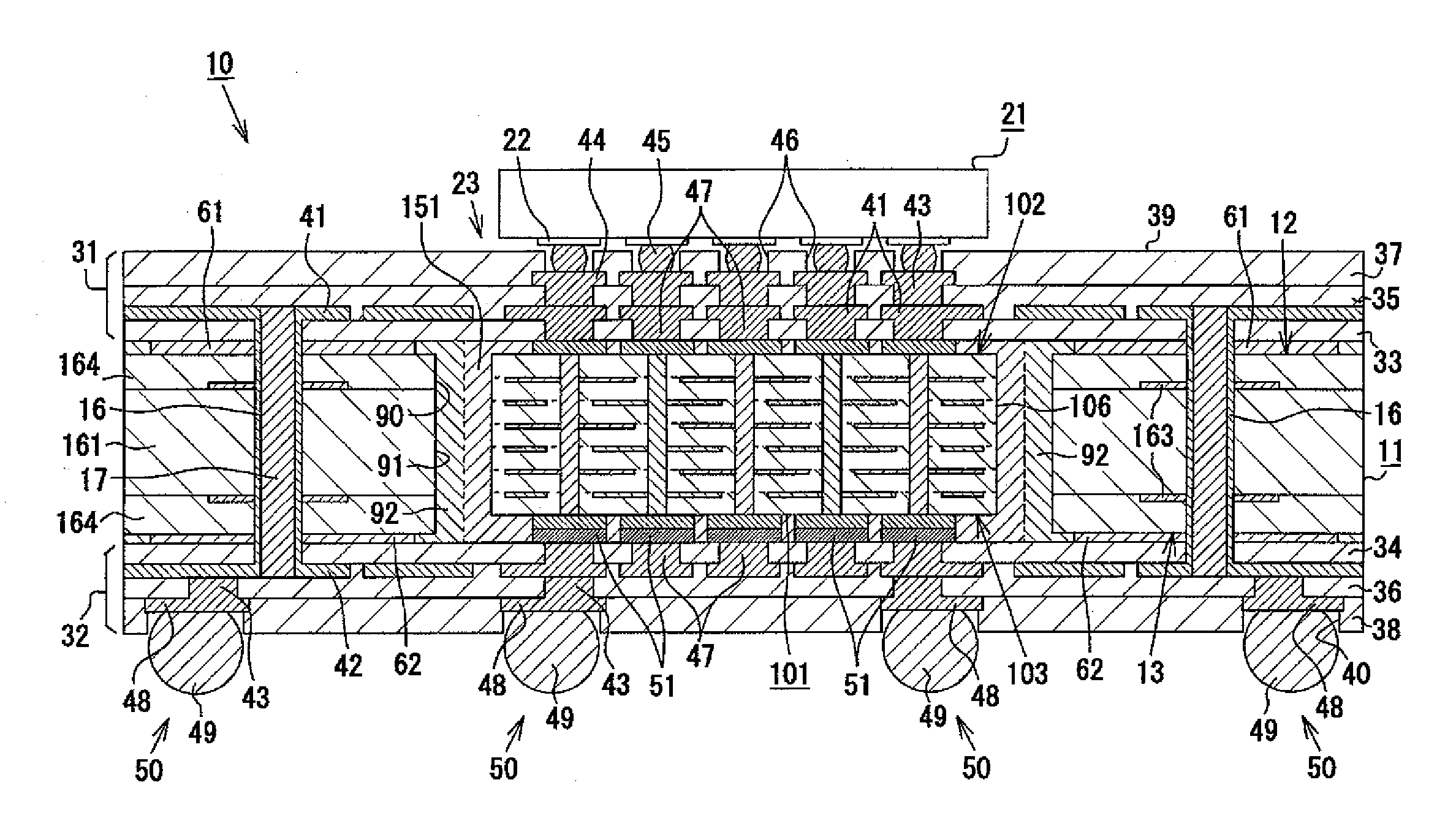
[0104]A wiring board with built-in component according to an embodiment of the present invention will be described in detail with reference to the drawings.
[0105]Referring to FIG. 1, there is shown a wiring board with built-in component 10 (hereinafter referred to as a “wiring board”). According to the illustrated embodiment, wiring board 10 is a wiring board for mounting an IC chip. The wiring board 10 is comprised of a rectangular plate-like core board 11, a main surface side buildup layer 31 (main surface side laminated wiring portion) formed on a core main surface 12 of the core board 11 (upper surface in FIG. 1) and a rear surface side buildup layer 32 (rear surface side laminated wiring portion) formed on a rear surface 13 of the core board 11 (lower surface in FIG. 1).
[0106]The main surface side buildup layer 31 formed on the core main surface 12 of the core board 11 has a structure in which two main surface side resin insulating layers 33 and 35 made of thermosetting resin (...
PUM
| Property | Measurement | Unit |
|---|---|---|
| Thickness | aaaaa | aaaaa |
| Thickness | aaaaa | aaaaa |
| Diameter | aaaaa | aaaaa |
Abstract
Description
Claims
Application Information