Semiconductor Device, Manufacturing Method Thereof, and Measuring Method Thereof

a technology of semiconductor devices and manufacturing methods, applied in the direction of individual semiconductor device testing, semiconductor/solid-state device testing/measurement, instruments, etc., can solve the problems of difficult measurement of properties, difficult method use, and pricking of teg manufactured over flexible substrates, etc., to achieve the effect of little deterioration

Inactive Publication Date: 2008-11-13
SEMICON ENERGY LAB CO LTD
View PDF38 Cites 72 Cited by
  • Summary
  • Abstract
  • Description
  • Claims
  • Application Information

AI Technical Summary

Benefits of technology

[0030]In a semiconductor device of the invention, a TEG which is sealed with first and second films having flexibility includes a terminal portion, and the terminal portion is connected to a wiring substrate having flexibility. Therefore, even in the TEG having flexibility, a contact-type test method can be used. Further, since an electrode pad is not used, deformation of the electrode pad does not occur and damages to the TEG are not generated due

Problems solved by technology

In a case of measuring a TEG manufactured over a flexible substrate, this method is difficult to be used.
In other words, since the flexible substrate is very soft, there is a problem in pricking the TEG manufactured over a flexible substrate when the probe contacts.
Accordingly, a bending property and a pulling property of the wireless chip are required to be measured with the TEG; however, such properties are difficult

Method used


Image

  • Semiconductor Device, Manufacturing Method Thereof, and Measuring Method Thereof
  • Semiconductor Device, Manufacturing Method Thereof, and Measuring Method Thereof
  • Semiconductor Device, Manufacturing Method Thereof, and Measuring Method Thereof

Examples


embodiment mode 1

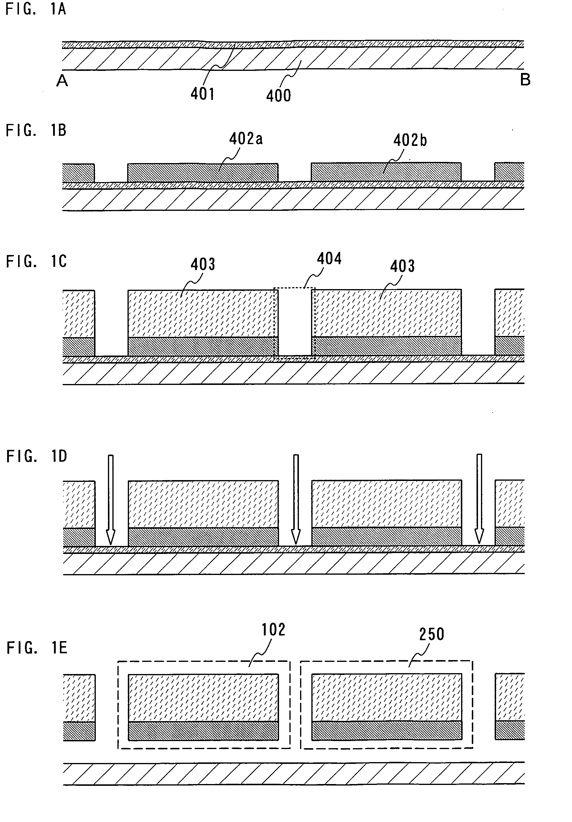
[0056]In Embodiment Mode 1, an example of a process will be explained, in which a chip for a TEG is manufactured at the same time as a plurality of wireless chips is manufactured over a flexible substrate.

[0057]First, a peeling layer 401 is formed over a substrate 400 shown in FIG. 1A. Since the substrate used here is removed in a later step, it is not limited to a flexible substrate, and a glass substrate, a quartz substrate, a ceramic substrate, or the like can be used. Further, a metal substrate including stainless steel or a semiconductor substrate on which an insulating film is formed may be used.

[0058]Next, over the peeling layer 401, an element layer 402a which is a part of an element 102 to be a wireless chip shown in FIG. 1E is formed, while an element layer 402b which is a part of an element 250 to be a chip for a TEG shown in FIG. 1E is formed (see FIG. 1B). The element 102 to be a wireless chip mainly includes a thin film circuit having a transistor or the like, and an a...

embodiment mode 2

[0079]In Embodiment Mode 2, a chip for a TEG is manufactured at the same time as a plurality of wireless chips is manufactured over a flexible substrate, and an example of how a result of a characteristic evaluation or a defect analysis on the chip for a TEG is reflected, will be described.

[0080]In a case of obtaining an anticipated characteristic result by the characteristic evaluation or the defect analysis on the chip for a TEG, the wireless chips manufactured at the same time as the chip for a TEG is manufactured, can be shipped, as it is, as products. In this case also, after cutting a terminal portion of the chip for a TEG, an element layer is again sealed. Alternatively, after separating a wiring substrate having flexibility, an element layer is again sealed with a film. Accordingly, the chip manufactured as a chip for a TEG can be used as a wireless chip, and yield can be improved.

[0081]In a case where an anticipated response result cannot be obtained by the characteristic e...

embodiment 1

[0082]In Embodiment 1, a process up to forming a plurality of wireless chips and a chip for a TEG as explained in Embodiment Mode 1, will be described in more detail.

[0083]First, a substrate 400 is prepared and a peeling layer 401 is formed over the substrate 400 as shown in FIG. 1A. Specifically, a glass substrate such as barium borosilicate glass, or aluminoborosilicate glass, a quartz substrate, a ceramic substrate, or the like can be used as the substrate 400. Further, a metal substrate such as stainless steel or a semiconductor substrate provided with an insulating film on its surface may also be used. In addition, although a flexible substrate made from a synthetic resin such as plastic generally tends to have lower heat-resistance than that of the above-described substrate material, it can also be used as long as it can withstand a process temperature in the manufacturing process. The surface of the substrate 400 may be planarized by polishing using a CMP method or the like.

[...


PUM


Abstract

To provide a semiconductor device capable of being easily subjected to a physical test without deteriorating characteristics. According to a measuring method of a semiconductor device in which an element layer provided with a test element including a terminal portion is sealed with first and second films having flexibility, the first film formed over the terminal portion is removed to form a contact hole reaching the terminal portion; the contact hole is filled with a resin containing a conductive material; heating is carried out after arranging a wiring substrate having flexibility over the resin with which filling has been performed so that the terminal portion and the wiring substrate having flexibility are electrically connected via the resin containing a conductive material; and a measurement is performed.

Description

TECHNICAL FIELD[0001]The present invention disclosed in the present specification relates to a semiconductor device provided over a substrate having flexibility, a manufacturing method thereof, and a measuring method thereof. Specifically, the invention relates to a TEG which performs a test of a wireless chip, such as a characteristic evaluation or a defect analysis.BACKGROUND ART[0002]Recently, a wireless chip which sends and receives data has been actively developed, and such a wireless chip is also called an IC tag, an ID tag, a radio frequency (RF) tag, a radio frequency identification (RFID) tag, a wireless tag, an electronic tag, a wireless processor, a wireless memory, or the like.[0003]As a transmission system of the wireless chip, there are three types of an electromagnetic coupling system, an electromagnetic induction system, and a radio wave system. The electromagnetic coupling system employs a mutual induction of electric coils by alternating magnetic field, and employs...

Claims


Application Information

Patent Timeline
IPC IPC(8): H01L23/58G01R31/26H01L21/00
CPCG01R31/2822G01R31/2884H01L22/34H01L23/66H01L2924/0002H01L2223/6677H01L2924/00H01L21/6835H01L21/78H01L22/14H01L2221/68359G01R31/2601G01R31/2607
Inventor TSURUME, TAKUYAASANO, ETSUKO
Owner SEMICON ENERGY LAB CO LTD
Why Eureka
Try Eureka