Semiconductor memory device

a memory device and semiconductor technology, applied in the direction of information storage, static storage, digital storage, etc., can solve the problems of increasing the coupling noise increasing the coupling capacitance between the bit lines, so as to shorten the local bit line length, reduce the coupling capacitance between adjacent local bit lines, and high-density semiconductor memory devices

Active Publication Date: 2008-11-13
LONGITUDE LICENSING LTD
View PDF6 Cites 10 Cited by
  • Summary
  • Abstract
  • Description
  • Claims
  • Application Information

AI Technical Summary

Benefits of technology

[0009]An object of the present invention is to provide a semiconductor memory device in which a hierarchical memory cell array is configured for higher integration of memory cells connected to local bit lines so as to suppress an increase in chip area, and coupling noise caused by coupling capacitance between bit lines is suppressed so as to obtain sufficient operating margin.
[0011]According to the semiconductor memory device of the present invention, in a hierarchical memory cell array, the local bit lines each partitioned into N sections along the global bit line are arranged, a signal read out from a memory cell formed at an intersection of the word line and the local bit line is amplified by the local sense amplifier through the local bit line, and the signal is further transmitted to the global bit line so as to be coupled to the external data line. Thus, when employing the cylindrical capacitor structure, the coupling capacitance between adjacent local bit lines can be reduced by shortening the length of the local bit lines. Thereby, the coupling noise is reduced so as to secure reading performance for the memory cell, and an increase in chip area can be suppressed in the semiconductor memory by arranging memory cells with high density.
[0021]As described above, according to the present invention, by employing a hierarchical memory cell array, the entire semiconductor memory device is configured by arranging local bit lines each partitioned into N sections along the global bit line, and the cylindrical capacitor structure is employed in each memory cell to achieve a high-density semiconductor memory device. Thereby, the coupling capacitance between adjacent local bit lines can be reduced by shortening the length of the local bit lines. Accordingly, the influence of the coupling noise can be suppressed so that the quality of a read signal is improved, and excellent operating margin Is achieved. Further, memory cells having a small size as 4F2 can be achieved using the cylindrical capacitor structure and the simple single-ended local sense amplifiers, and thus an increase in the entire chip area can be suppressed.

Problems solved by technology

However, since sides of cylinders of adjacent memory cells are arranged close to each other with a sufficient height when employing the conventional capacitor structure, the capacitance between the cylinders becomes relatively large.
Then, the capacitance between the cylinders occupies a larger part of a coupling capacitance between bit lines, which causes an increase in coupling noise between bit lines when reading a signal through a bit line.
Particularly, when many memory cells are connected to one bit line in a highly integrated memory cell array, the coupling capacitance between the bit lines accordingly increases, and influence of the coupling noise remarkably increases so that read operation is hindered.
In this manner, when employing the cylindrical capacitor structure, it is a problem that operating margin decreases due to the coupling noise caused by the capacitance between the cylinders.

Method used


Image

  • Semiconductor memory device
  • Semiconductor memory device
  • Semiconductor memory device

Examples


Embodiment Construction

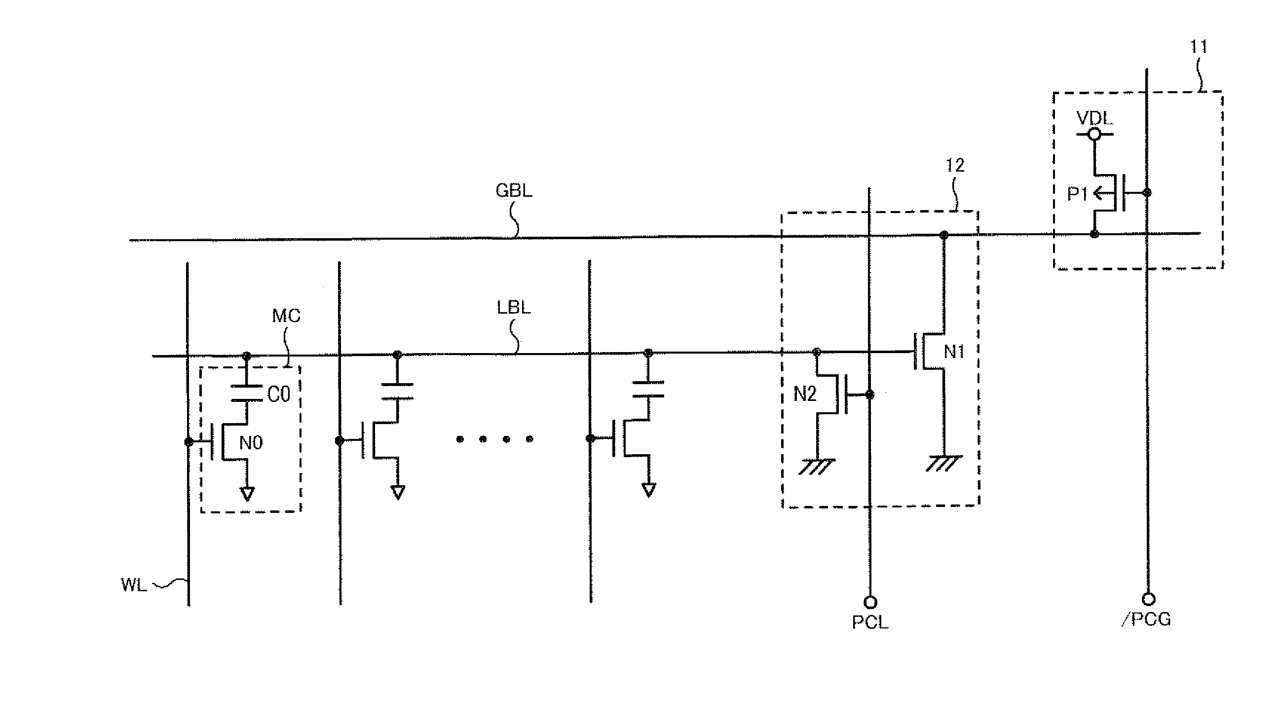
[0031]A preferred embodiment of the present invention will be described with reference to the accompanying drawings. In the following, an embodiment in which the present invention is applied to a DRAM having a hierarchical memory cell array as a semiconductor memory device will be described.

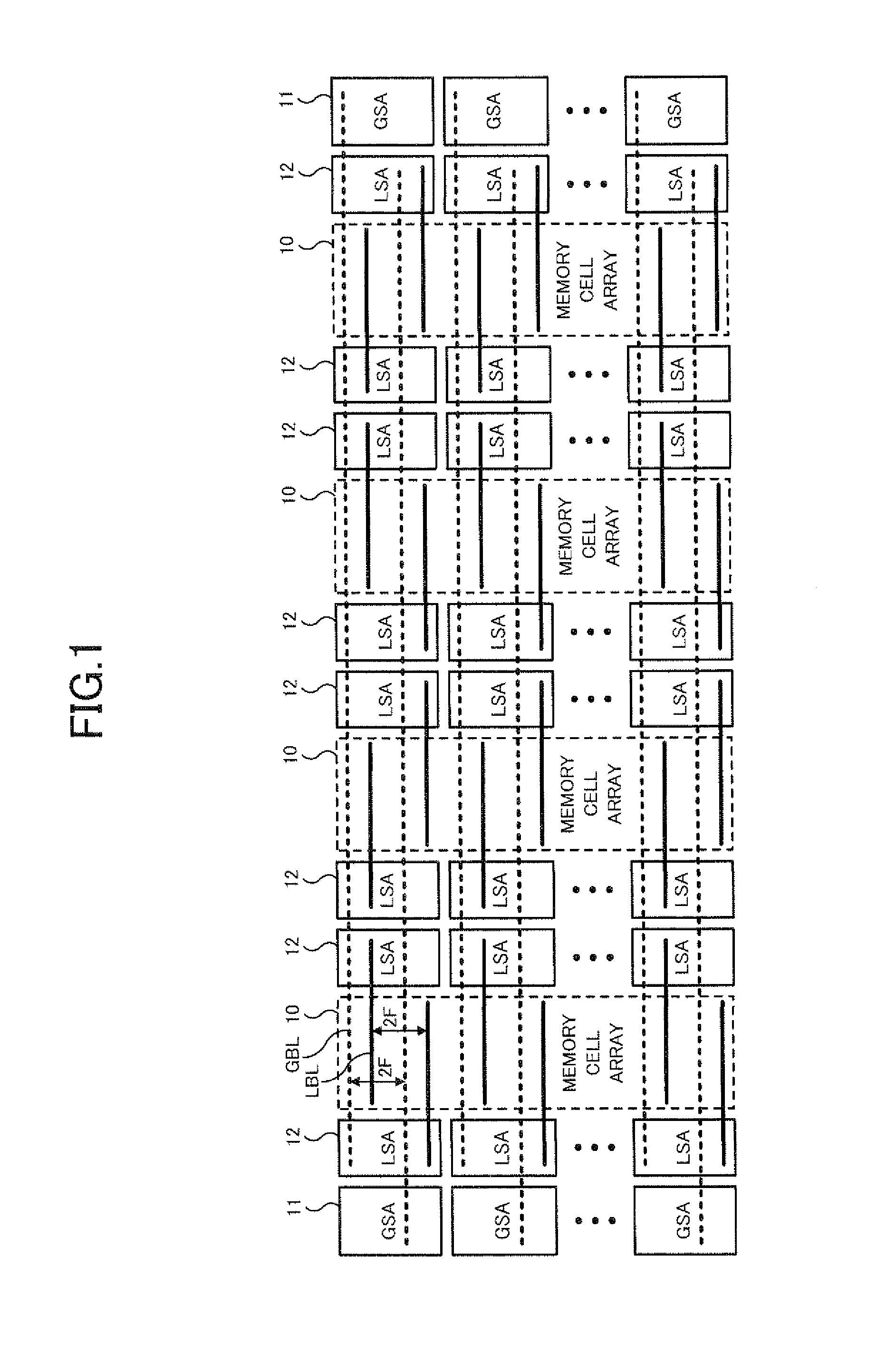
[0032]FIG. 1 shows an entire configuration of the DRAM of the embodiment. In FIG. 1, there are shown four memory cell arrays 10, a plurality of global sense amplifiers 11, a plurality of local sense amplifiers 12, a plurality of global bit lines GBL, and a plurality of local bit lines LBL.

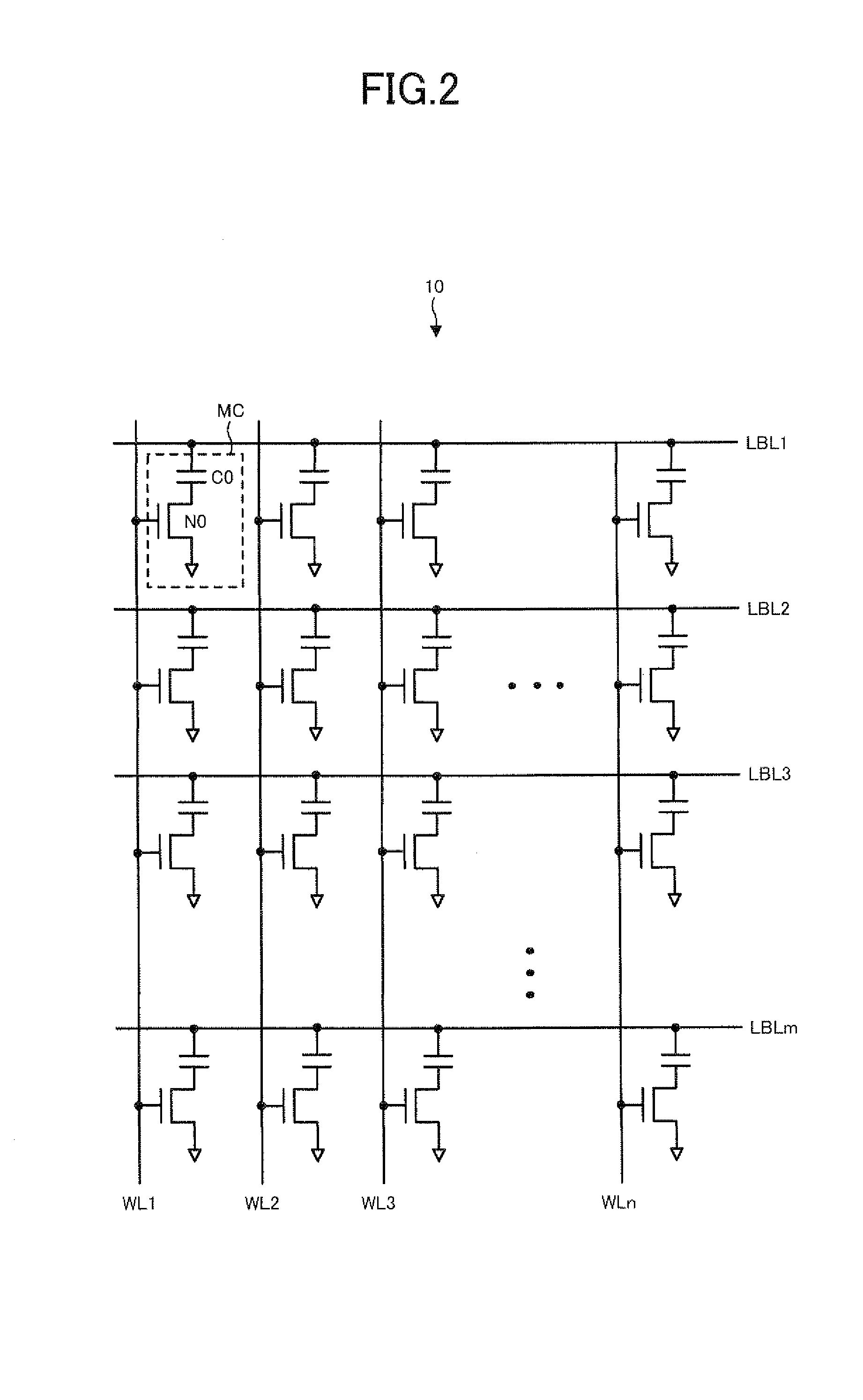
[0033]Each memory cell array 10 includes a large number of memory cells formed at all intersections of a plurality of word lines and the plurality of local bit lines LBL intersecting therewith. As shown in FIG. 1, the plurality of local his lines LBL is regularly aligned with a pitch 2F based on a design rule value F in a word line extending direction. Besides, the plurality of global bit lines GBL is also align...


PUM


Abstract

A semiconductor memory device comprises. word lines; global bit lines intersecting with the word lines; local bit lines partitioned into N (N is an integer greater than or equal to two) sections along the global bit lines and aligned with a same pitch as the global bit lines; N memory cell arrays each including memory cells each having cylindrical capacitor structure formed at intersections of the word lines and the local bit lines and being arranged corresponding to the sections of the local bit lines; local sense amplifiers for amplifying a signal read out from a selected memory cell to the local bit line and for outputting the signal to the global bit line; and global sense amplifiers for coupling the signal transmitted from the local sense amplifier corresponding to the selected memory cell through the global bit line to an external data line.

Description

BACKGROUND OF THE INVENTION[0001]1. Field of the Invention[0002]The present invention relates to a semiconductor memory device which rewritably stores data in a plurality or memory cells formed at intersections of a plurality of word lines and a plurality of bit lines, and particularly relates to a semiconductor memory device in which a memory cell array is configured so that an opposite electrode of a capacitor of each memory cell is directly connected to a bit line.[0003]2. Description of the Related Art[0004]Generally, a memory cell array of a DRAM includes a large number of memory cells formed at intersections of bit lines and word lines. Regarding the memory cell composed of one transistor and one capacitor, a structure in which an opposite electrode of the capacitor is directly connected to a bit line is proposed for the purpose of higher integration of the DRAM (e.g., see Patent References 1 to 3). On the premise of such a structure, when achieving a fine memory cell using a ...

Claims


Application Information

Patent Timeline
Patent Type & Authority Applications(United States)
IPC IPC(8): G11C11/24G11C7/00
CPCG11C7/02G11C11/4094G11C11/4097G11C2207/002
Inventor KAJIGAYA, KAZUHIKO
Owner LONGITUDE LICENSING LTD
Why Eureka
Try Eureka